The D flip flop is the most important flip flop in digital electronics. The both inputs of the flip flop. S & R, can never be equal one at the same time. To get this , we use a gated SR FF with an inverter between the inputs.
In digital electronics, a flip flop is a logic circuit that is used to store 1 bit of binary information. Therefore, the flip-flops are considered fundamental building block of digital storage devices.
Based on construction and design, several different types of flip-flops(FFs) are available such as SR , JK, T , and D FF. In this article, we will discuss D FF, its truth table, circuit diagram, and applications.
What is a D Flip Flop?
The D flip flop have only one input line D and two output lines Q and Q’. It also has a clock input line for triggering of the circuit.
The logic block diagram is shown in the following figure.
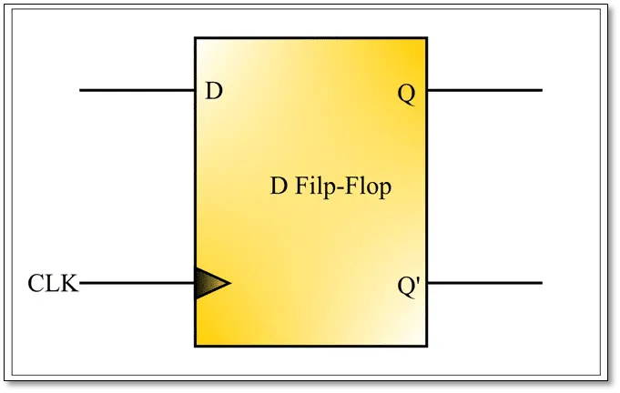
Here, it has an input line designated by the symbol D, where a binary input is applied. Another input line to the D FF is a clock signal, denoted by CLK. The signal is utilized to synchronize and trigger the flip-flop. The output Q is the normal output which determines the state of the flip-flop, while the output Q’ is the complemented output which is inversion of the normal output Q.
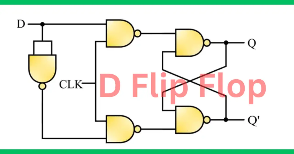
D Flip Flop Circuit Diagram
We can design a D FF using digital logic gates. The logic circuit diagram of a D flip-flop is shown below.
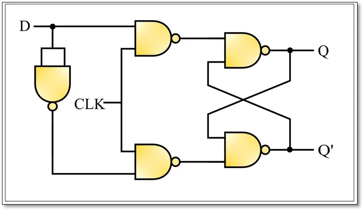
It is clear that we can design a D flip-flop by using five NAND gates. It is basically a NAND logic SR FF in which S is directly connected to D input and the R is connected to the D input through an invert gate.
Truth Table of D Flip-Flop
Truth table provides information about its operation for different values of input D. The truth table of D FF is shown in the below table.
| Input (D) | Next State (Qn+1) | Comment |
| 0 | 0 | Reset |
| 1 | 1 | Set |
From the truth table of D flip-flop, it is clear that when the value of the input D is logic 0, the D FF enters to the reset state, and when the input D is logic 1, the FF goes into the set state.
Characteristic Table of D Flip-Flop
The characteristic table of a D FF provides information about transition of state as per the input signal. The characteristic table is given below:
| Input (D) | Previous State (Qn) | Next State (Qn+1) |
| 0 | 0 | 0 |
| 0 | 1 | 0 |
| 1 | 0 | 1 |
| 1 | 1 | 1 |
Characteristic Equation of D Flip Flop
We can use K-Map and characteristic table of D FF to derive its characteristic equation.
The K-map simplification of the characteristic table is shown below.
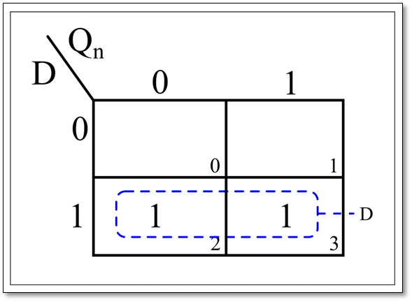
From the K-map simplification, we get the following expression as the characteristic equation.

Benefits
The following are some major advantages of D flip flop.
- It is simpler to design and use in digital circuits, as it has only one input line.
- It does not have the problem of race condition due to absence of feedback loop.
- It does not have any invalid state.
- It consumes less power.
Applications
Some common applications of D FF are listed below:
- Used in shift registers in digital systems.
- Used to introduce a delay in a digital system.
- Also used to design state machines.
- For designing binary counters.
This is all about D flip-flop, its truth table, and applications. The D FF is a very simple circuit used to store binary information in digital systems.