In digital electronics, the OR Gate is a fundamental logic gate used to perform logical OR operations on binary inputs. It plays a key role in digital systems by producing an output based on input conditions and is widely used in logic circuits and control applications.
In this article, we will learn about the logic OR gate, including its definition, symbol, logical expression, truth table, types, circuit diagram, IC numbers, and real-world implementation. Let’s begin with the basics of the OR gate.
OR Gate – Definition, Inputs and Basic Concept
In digital electronics, an OR gate is a fundamental logic gate that produces a HIGH (1) output when any one or more of its inputs are HIGH (1). The output becomes LOW (0) only when all inputs are LOW (0). This behavior is based on the logical OR operation, where input signals are combined to generate a single output.
For example, in a simple lighting system with two switches, turning either switch ON will activate the light. Similarly, in an alarm system, if any one sensor detects a fault, the alarm is triggered. These real-world cases reflect the working principle of the OR gate.
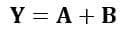
The Boolean expression of an OR gate is Y = A + B, where ‘+’ represents the logical OR operation, A and B are inputs and Y is output. This expression can also be extended for multiple inputs in digital systems.
OR gates are available in 2-input, 3-input, and multi-input configurations depending on circuit requirements. They are widely used in digital systems, decision-making circuits, and automation applications as basic building blocks.
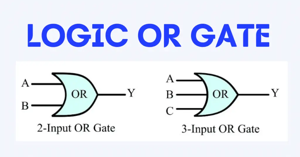
OR Gate Symbol
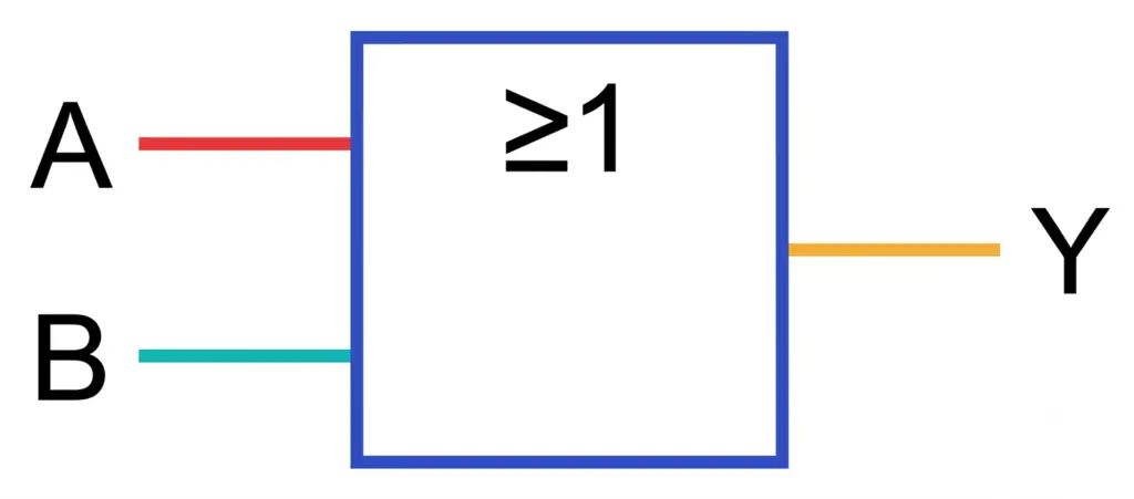
There are two commonly used representations of the OR gate symbol: the ANSI (American or MIL) symbol and the IEC (European rectangular) symbol. The DIN symbol is now considered deprecated in modern digital electronics. ANSI symbols are commonly used in North American ANSI standard logic diagrams, while IEC symbols are used in European standards.
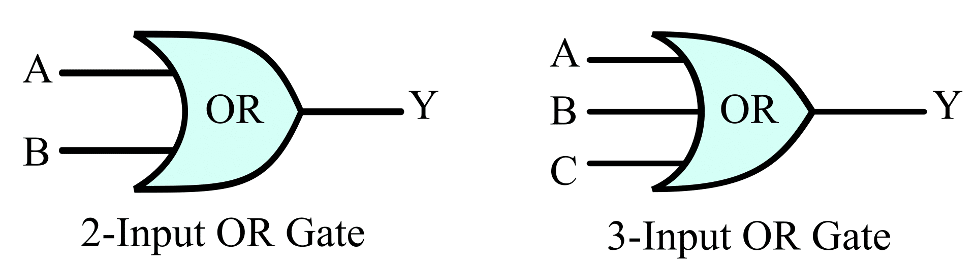
The OR Gate symbol of two-input and three-input configurations as per ANSI standard are depicted in the following figure.
In contrast, in the IEC symbol, the notation “≥1” indicates that the output becomes HIGH when at least one input is active.
The symbol helps quickly identify how inputs combine to produce an output in digital circuits.
Types of OR Gate
OR gates are generally classified into three main types: 2-input OR gate, 3-input OR gate, and multi-input OR gate. All of these follow the same fundamental OR logic operation.
2-Input OR Gate
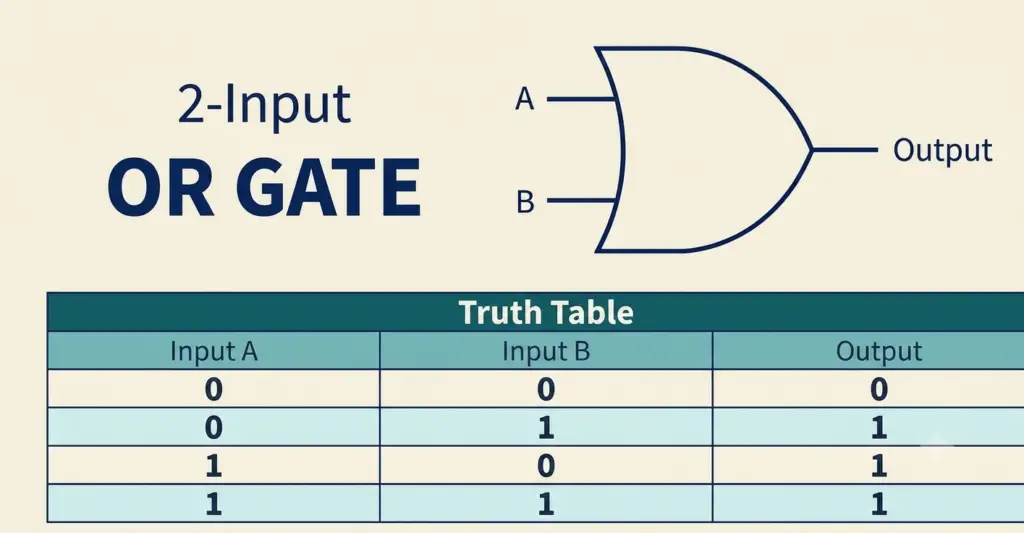
A 2-input OR gate gives HIGH (1) output when any one of the inputs is HIGH (1). Only when both inputs are LOW (0), the output becomes LOW (0).
Logical Expression of 2-Input OR Gate
The operation of the OR gate is represented by the ‘+’ symbol, , which denotes the logical OR (addition) operation in Boolean algebra.
The logical expression of a two-input OR gate is given by,
Where A and B are the input variables, and Y is the output variable of the OR gate.
2- Input OR Gate Operation
A 2-input OR gate is the simplest form of OR gate. It accepts two binary inputs and produces a single output. The output becomes HIGH (1) when at least one of the inputs is HIGH (1). The total number of input combinations is two raised to the power of two, which equals four (2² = 4). It performs the Boolean operation Y = A + B.
The operation of a two-input OR gate for different input combinations is described as follows:
- When A = 0 and B = 0 → Y = 0
- When A = 0 and B = 1 → Y = 1
- When A = 1 and B = 0 → Y = 1
- When A = 1 and B = 1 → Y = 1
Truth Table of 2- Input OR Gate
The truth table of a two-input OR gate is given below. It shows all possible input combinations and their corresponding outputs.
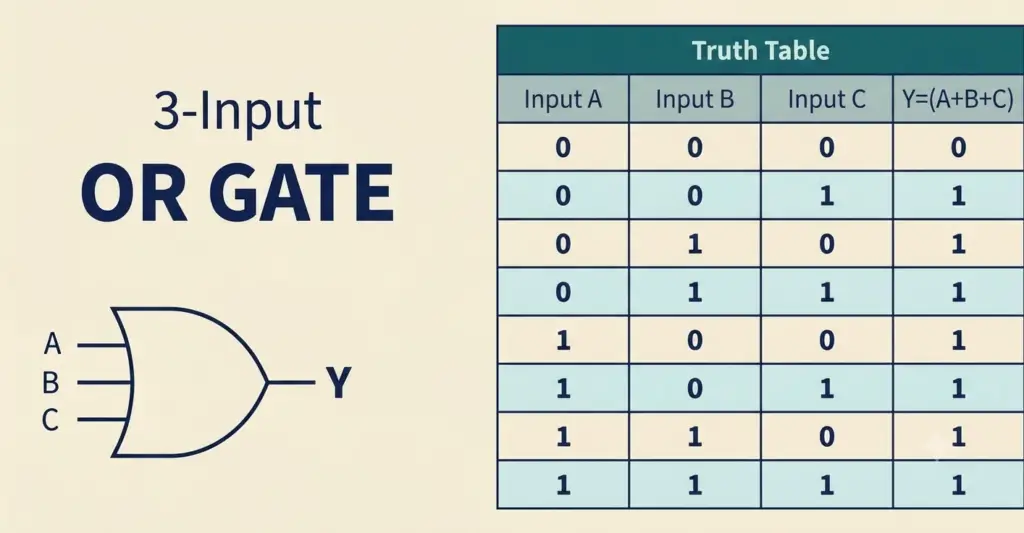
3-Input OR Gate
A 3-input OR gate gives HIGH (1) output when any one of the inputs is HIGH (1). Only when all inputs are LOW (0), the output becomes LOW (0).
Logical Expression of 3-Input OR Gate
The logical expression of a three-input OR gate is given by,
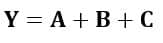
Where, A, B, and C are the three input variables and Y is the output variable of the logic OR gate.
3- Input OR Gate Operation
An OR gate can also be designed with multiple inputs beyond two inputs. When several OR gates are connected in a cascading form, they can handle higher numbers of inputs efficiently. In a three-input OR gate, all input combinations are based on binary logic, resulting in a total of two raised to the power of three possible combinations, which equals eight (2³ = 8). The Boolean expression for a three-input OR gate is X = A + B + C.
The operation of a three-input OR gate for different possible input combinations is described below:
- When A = 0, B = 0, C = 0 → Y = 0
- When A = 0, B = 0, C = 1 → Y = 1
- When A = 0, B = 1, C = 0 → Y = 1
- When A = 0, B = 1, C = 1 → Y = 1
- When A = 1, B = 0, C = 0 → Y = 1
- When A = 1, B = 0, C = 1 → Y = 1
- When A = 1, B = 1, C = 0 → Y = 1
- When A = 1, B = 1, C = 1 → Y = 1
Truth Table of 3-Input OR Gate
The table showing the relationship between inputs and output of a 3-input logic OR gate is referred to as its truth table.
Multi-Input OR Gate
A multi-input OR gate is an extension of the basic OR gate that can accept more than two inputs and produce a single output based on OR logic.
In practice, the logic OR gate is mainly implemented for having two-inputs, three-inputs, and four-inputs.
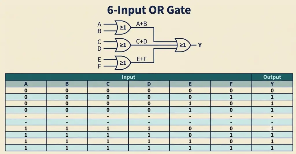
However, we can implement a higher-order logic OR gate using multiple lower-order logic OR gates. For example, the following figure specifies a logic OR gate of 6 inputs using four 2-input OR gates.
For an n-input OR gate, the Boolean expression is: Y = A₁ + A₂ + A₃ + … + Aₙ
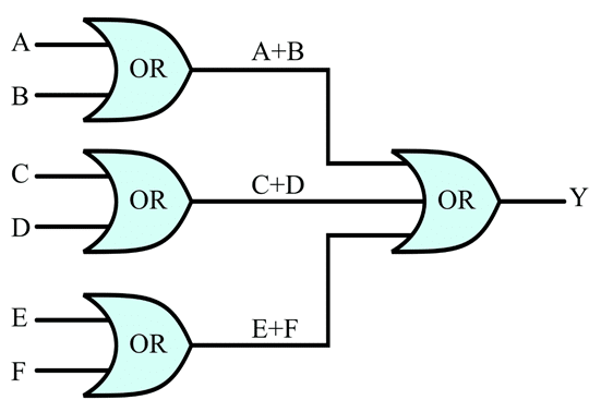
The logical expression of the above circuit of 6-input OR gate is as,
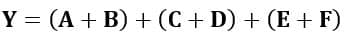
The following diagram illustrates the logic circuit and truth table for a 6-input OR gate. By cascading multiple 2-input OR gates, we can determine the final output Y based on inputs A through F.
Implementation of Two-Input OR Gate in Resistor-Transistor Logic
A two-input OR gate can be implemented using NPN transistors in Resistor-Transistor Logic (RTL), where the output becomes HIGH if either transistor is switched ON. In this circuit, the transistors act as electronic switches controlled by the input signals. If at least one input is HIGH, the corresponding transistor conducts and produces a HIGH output. The output becomes LOW only when all inputs are LOW, which satisfies the fundamental operating principle of an OR gate.
Circuit Diagram of 2-input OR Gate Using Transistors
The following figure depicts the realization of a two-input OR gate in RTL (Resistor Transistor Logic).
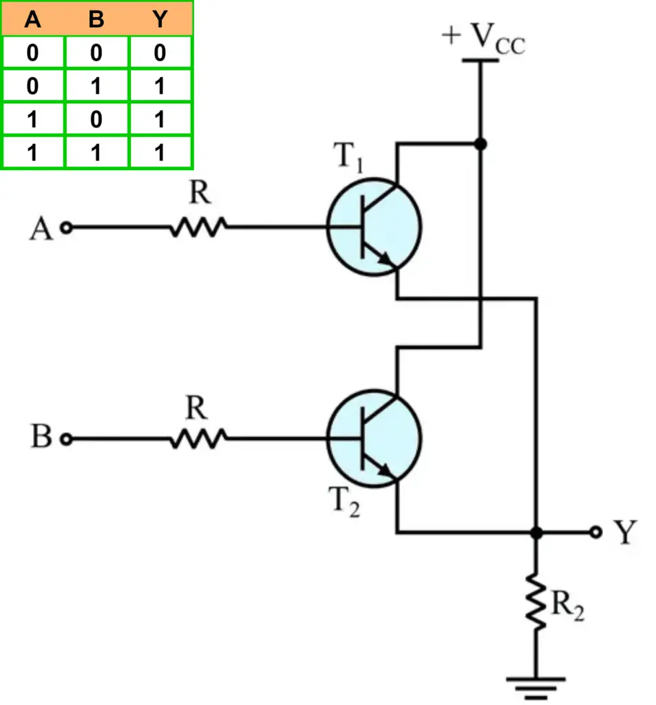
Working of the Circuit
The circuit operates based on transistor switching, where each input controls a transistor acting as an electronic switch. The resistor R2 acts as the load resistor in the RTL OR gate circuit. When either transistor conducts, a voltage develops across R2, producing a HIGH output. When both transistors are OFF, no current flows through R2 and the output remains LOW. Thus, R2 plays an important role in developing the output voltage and ensuring proper logic-level operation.
- When both inputs A and B are zero, transistor T1 and T2 remain in the OFF state. Therefore, no collector current flows through the transistors, and emitter current IE is zero. As a result, the drop across resistance R2 (IER2) is zero, and the output voltage Y remains 0 V. Hence, the output is 0 when A = 0 and B = 0.
- When A = 0 and B = 1, transistor T2 turns ON and conducts. This produces a voltage drop across resistor R2 , which is approximately equal to the supply voltage., resulting in a HIGH output (Y = 1).
- When A = 1 and B = 0, transistor T1 turns ON and conducts, producing a HIGH output (Y = 1).
- When A = 1 and B = 1, both transistors T1 and T2 conduct simultaneously. Therefore, the output remains HIGH (Y = 1).
Therefore, the output is HIGH whenever at least one input is HIGH and LOW only when all inputs are LOW, which matches the truth table of an OR gate.
Operation Summary of RTL OR Gate
The following table summarizes the operation of the RTL OR gate for all possible input combinations and shows the corresponding transistor states and output levels.
| Input A | Input B | T1 State | T2 State | Output Y |
| 0 | 0 | OFF | OFF | 0 |
| 0 | 1 | OFF | ON | 1 |
| 1 | 0 | ON | OFF | 1 |
| 1 | 1 | ON | ON | 1 |
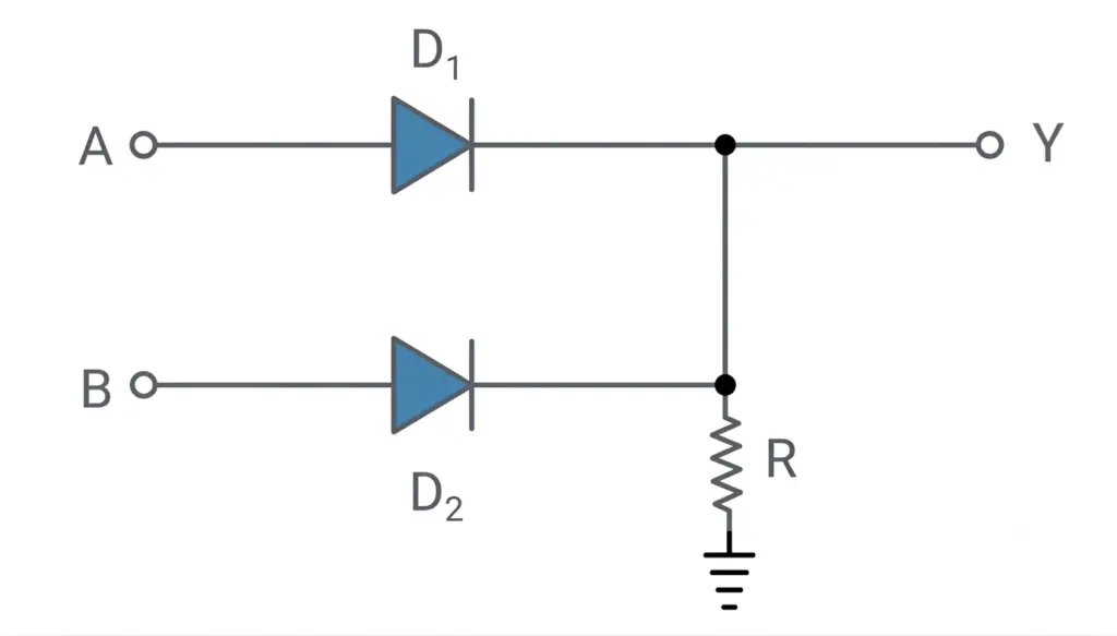
OR Gate Using Diode Resistor Logic
A simple OR gate can be implemented using two diodes and a resistor. This circuit performs the same logical OR operation as a digital OR gate, where the output becomes HIGH when any one of the inputs is HIGH.
Circuit Operation
In the diode OR gate circuit, the anodes of the diodes are connected to the input terminals A and B, while their cathodes are connected together at the output terminal Y. A resistor is connected between the output and ground to provide a LOW state when no input signal is present. The OR Gate diode circuit diagram is shown below:
Case 1: A = 0 V and B = 0 V
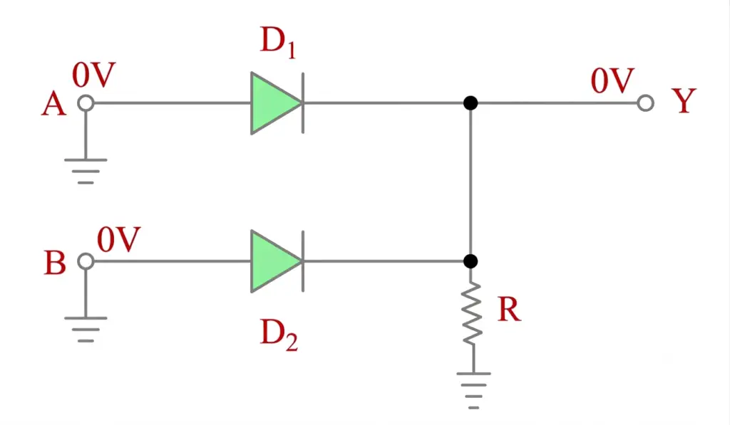
When both inputs are at 0 V, neither diode is forward biased. As a result, no current flows through the circuit, and the pull-down resistor keeps the output terminal at 0 V. Therefore, the output is considered Logic 0.
Case 2: A = 5 V and B = 0 V
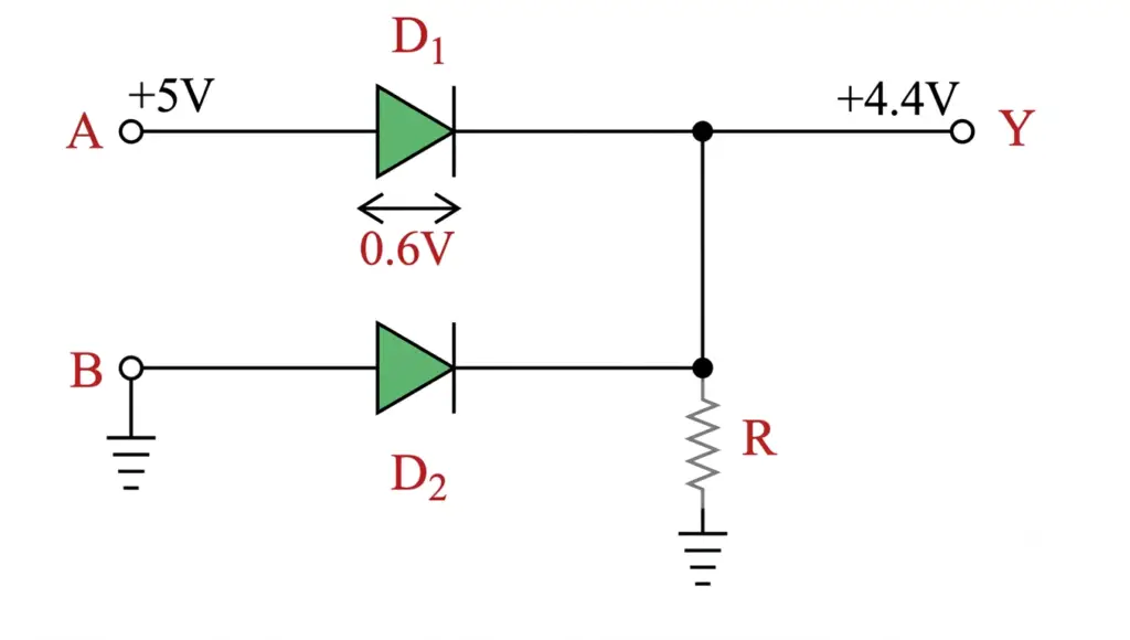
When input A is HIGH, the diode connected to A becomes forward biased and starts conducting. Current flows through the diode to the output terminal, causing the output voltage to rise. Since silicon diodes have a forward voltage drop of approximately 0.7 V, the output voltage becomes approximately:
Y = 5 V − 0.7 V = 4.3 V
This voltage level is recognized as Logic 1 in digital circuits.
Case 3: A = 0 V and B = 5 V
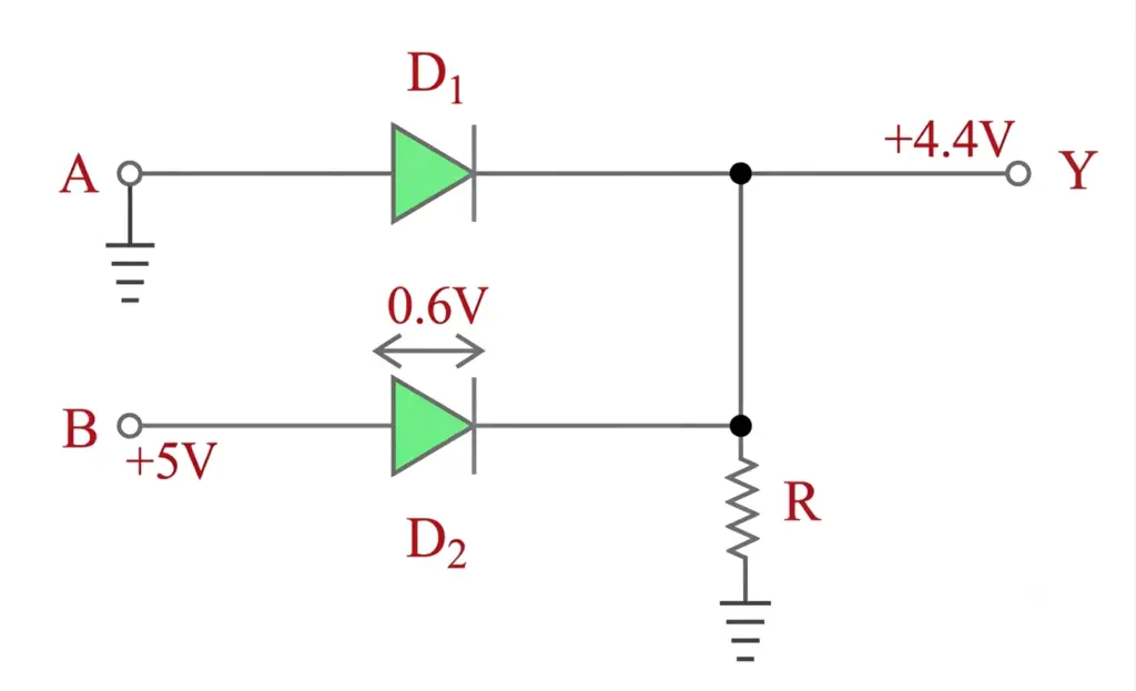
In this condition, the diode connected to input B becomes forward biased while the other diode remains reverse biased. The output voltage again rises to approximately 4.3 V, producing a Logic 1 at the output.
Case 4: A = 5 V and B = 5 V
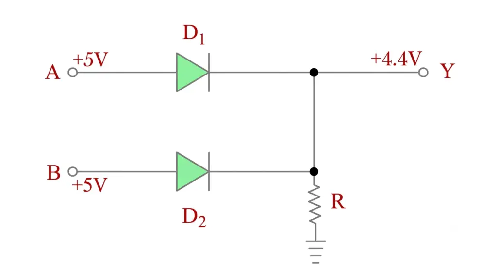
When both inputs are HIGH, both diodes conduct simultaneously. The output voltage remains close to 4.3 V due to the forward voltage drop across the diodes. Since at least one input is HIGH, the output remains Logic 1.
OR Gate Diode Circuit Operation Summary
The following table summarizes the operation of the diode OR gate for all possible input combinations. It shows which diode conducts, the approximate output voltage produced, and the corresponding logic output. From the table, it is clear that the output becomes HIGH whenever at least one input is HIGH, which is the fundamental operating principle of an OR gate.
| Input A | Input B | Conducting Diode(s) | Output Voltage (Approx.) | Logic Output |
| 0 V | 0 V | None | 0 V | 0 |
| 5 V | 0 V | D1 | ≈ 4.3 V | 1 |
| 0 V | 5 V | D2 | ≈ 4.3 V | 1 |
| 5 V | 5 V | D1 and D2 | ≈ 4.3 V | 1 |
Electrical Equivalent Circuit of OR Gate
The electrical equivalent circuit of a two-input OR gate is shown in the following figure.
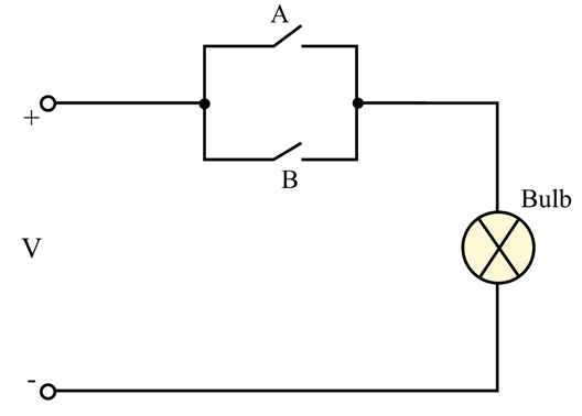
In this circuit, when both switches, i.e. A and B are open, the bulb will not glow. If any of the switches is closed or both switches are closed, the bulb will glow.
OR Gate Integrated Circuits (ICs)
OR gates are commercially available as integrated circuits (ICs) in both TTL (Transistor-Transistor Logic) and CMOS (Complementary Metal-Oxide-Semiconductor) families. These ICs contain multiple OR gates within a single package, making them suitable for digital circuit design and logic applications.
The most commonly used OR gate ICs include 74LS32 in the TTL family and CD4071, CD4075, and CD4072 in the CMOS family. These ICs differ in terms of the number of gates and inputs available per gate.
The commonly available OR gates in the form of integrated circuits are as follows:
OR Gate IC 4071
The 74LS32 is a TTL-based integrated circuit that contains four independent 2-input OR gates in a 14-pin package. The suffix LS stands for Low-Power Schottky, indicating lower power consumption and faster switching performance compared to standard TTL devices.
The pinout diagram of 74LS32 is given below.
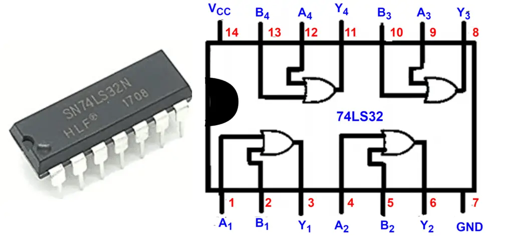
Pin Configuration:
- Pin 14 → VCC (+Supply)
- Pin 7 → GND (Ground)
- Pin 1, 2 → Inputs | Pin 3 → Output (Gate 1)
- Pin 4, 5 → Inputs | Pin 6 → Output (Gate 2)
- Pin 9, 10 → Inputs | Pin 8 → Output (Gate 3)
- Pin 12, 13 → Inputs | Pin 11 → Output (Gate 4)
OR Gate IC CD4071
The CD4071 is a CMOS logic IC that incorporates four 2-input OR gates within a single 14-pin package. Due to CMOS technology, the IC offers low power consumption, high noise immunity, and a wider operating voltage range than TTL devices.
The pinout diagram of CD4071 is given below.
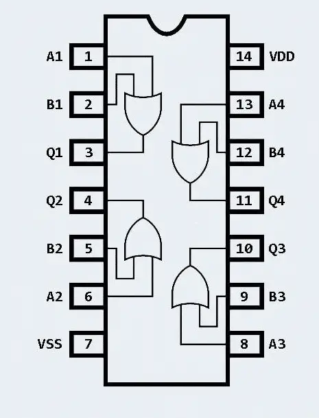
Pin Configuration:
- Pin 14 → VDD (+Supply)
- Pin 7 → VSS (Ground)
- Pin 1, 2 → Inputs | Pin 3 → Output (Gate 1)
- Pin 5, 6 → Inputs | Pin 4 → Output (Gate 2)
- Pin 8, 9 → Inputs | Pin 10 → Output (Gate 3)
- Pin 12, 13 → Inputs | Pin 11 → Output (Gate 4)
OR Gate IC CD4075
The CD4075 is a CMOS integrated circuit that contains three independent 3-input OR gates in a single package. It is commonly used in digital circuits where multiple input signals need to be combined using OR logic. The IC offers low power consumption, high noise immunity, and reliable operation, making it suitable for logic control, automation, and signal processing applications.
The pinout diagram of CD4075 is given below.
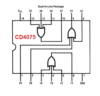
Pin Configuration:
- Pin 14 → VDD (+Supply)
- Pin 7 → VSS (Ground)
- Pin 1, 2, 8 → Inputs | Pin 9 → Output (Gate 1)
- Pin 3, 4, 5 → Inputs | Pin 6→ Output (Gate 2)
- Pin 11, 12, 13 → Inputs | Pin 10 → Output (Gate 3)
OR Gate IC CD4072
The CD4072 is a CMOS logic IC that consists of two independent 4-input OR gates. It is designed for applications that require OR operations involving multiple input signals. Due to CMOS technology, the IC provides low power dissipation and excellent noise immunity, making it ideal for digital control systems, alarm circuits, and industrial automation applications.
The pinout diagram of CD4072 is given below.
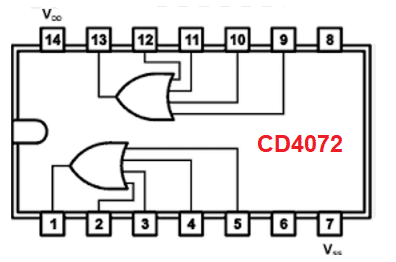
Pin Configuration:
- Pin 14 → VDD (+Supply)
- Pin 7 → VSS (Ground)
- Pin 1, 2. 3. 4 → Inputs | Pin 1 → Output (Gate 1)
- Pin 9, 10, 11, 12 → Inputs | Pin 13 → Output (Gate 2)
Summary of OR Gate ICs
| IC Number | Configuration | Inputs | Description |
| 74LS32 | TTL, Quad | 2 | Four independent 2-input gates for TTL logic applications. |
| CD4071 | CMOS, Quad | 2 | Low-power CMOS device with four 2-input gates. |
| CD4075 | CMOS, Triple | 3 | Three independent 3-input gates in a single package. |
| CD4072 | CMOS, Dual | 4 | Two independent 4-input gates for multi-input logic operations. |
Applications of OR Gate
- Smart Irrigation Systems: Logic OR gates can be used to automate irrigation. If any sensor detects dryness in the soil, the output activates the watering system.
- Home Automation Controls: OR gates combine signals from multiple sensors or switches. For instance, if any room’s motion sensor is triggered, lights or HVAC systems can be turned on automatically.
- Emergency Systems: In buildings or facilities, OR gates can control emergency lighting or alarms. If any connected switch or sensor detects a fault, the system activates the necessary response.
- Industrial Monitoring: OR gates are employed in machinery to monitor multiple conditions. If any safety parameter is violated, the machine can automatically stop or signal an alert.
- General Use: OR gates are widely used in decision-making circuits where the output depends on whether any one of multiple input conditions is satisfied.
Advantages of OR Gate
OR gates provide several important benefits in digital circuit design due to their simplicity and wide usability.
- Simple Design: OR gates have a straightforward design, making them easy to understand and implement in circuits.
- Versatile Usage: They can handle multiple inputs, which makes them suitable for a wide variety of digital applications.
- Foundational Component: OR gates serve as the building blocks of complex integrated circuits, enabling the creation of other logic functions like NAND gate, NOR gate, XOR gate and XNOR gate .
- Efficient Logic Implementation: They allow designers to implement decision-making processes effectively, checking if at least one condition is met.
Disadvantages of OR Gate
Although OR gates are widely used in digital systems, they also have certain limitations in practical applications.
- Limited Output Detail: OR gates only indicate if any input is high; they do not reveal which specific input triggered the output.
- Not Suitable for Precision Tasks: Applications that require exact input tracking may not benefit from OR gates, since the output is binary.
- Non-Invertible Nature: The output remains high if any input is high, which may limit certain logic designs that require inversion.
- Higher Power in Complex Circuits: Compared to simpler gates like NOT or AND, using OR gates in complex networks can increase power consumption.
Conclusion
OR gates are essential components in digital electronics. They simplify decision-making by producing a HIGH (1) output when any input condition is satisfied. From smart home systems to industrial monitoring and emergency setups, OR gates play a key role in designing both simple and complex digital circuits. Understanding their operation, symbol, truth table, and implementation is important for anyone working in digital electronics and logic design.
Frequently Asked Questions (FAQs) on OR Gate
An OR gate is a basic logic gate that produces a HIGH (1) output when any one or more of its inputs are HIGH (1). The output becomes LOW (0) only when all inputs are LOW (0).
The Boolean expression of a 2-input OR gate is:
Y = A + B
Here, “+” represents the logical OR operation. For multiple inputs, it can be written as:
Y = A + B + C + …
An OR gate gives output LOW (0) only when all inputs are 0. In all other cases, the output is HIGH (1):
0 + 0 = 0
0 + 1 = 1
1 + 0 = 1
1 + 1 = 1
OR gates are used in systems where any one condition should activate the output, such as:
-Alarm systems
-Home automation
-Security systems
-Industrial control systems
-Smart irrigation systems
A 3-input OR gate produces a HIGH output when any one of its three inputs is HIGH. It gives LOW output only when all inputs are LOW. Its Boolean expression is:
Y = A + B + C
Related Articles:
- XNOR Gate: Symbol and Truth Table
- What is a NOT Gate? Logic Symbol and Truth Table
- Exclusive-OR Gate with EX-OR Gate Truth Table
- Universal Logic Gate: NAND Gate and NOR Gate as Universal Gate
- Logic NAND Gate- Symbol, Truth Table, Circuit Diagram, Working
- Logic AND Gate: Symbol, Truth Table, Working, Circuit Diagram
- Logic NOR Gate- Symbol, Truth Table and Circuit Diagram
- Logic Gates: Types, Working, Symbols, Truth Tables, Boolean Expressions