The PN junction diode is one of the most fundamental electronic components. It is a semiconductor device that can conduct current only in one direction. Hence, it is a unidirectional semiconductor device.
What is a PN Junction Diode?
As its name implies, a PN junction diode is one that is constructed by joining a P-type semiconductor material with an N-type semiconductor material.
Therefore, a PN junction diode is defined as a two-terminal electronic semiconductor device consisting of two layers of P and N-type semiconductors joined together, allowing current to flow only in one direction.
Construction of PN Junction Diode
The construction of a typical junction diode is shown in the following figure.
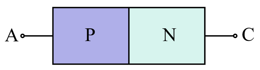
It consists of two layers, namely, P-type semiconductors and N-type semiconductors joined together. It has two metallic terminals namely, anode and cathode, connected to both ends of the diode.
A PN junction diode is typically constructed by using either Germanium or Silicon crystals. A PN junction is formed when an N-type semiconductor material is connected to a P-type semiconductor material. Actually, the formation of a PN junction involves highly specialized techniques like growth, alloying, and diffusion methods.
In the P-type semiconductor, the majority of charge carriers are holes, whereas electrons are the minority charge carriers. On the other hand, the N-type semiconductor has electrons as the majority charge carriers, whereas holes are the minority charge carriers.
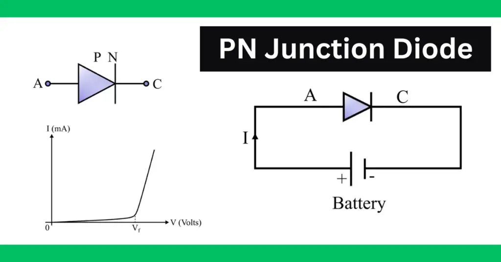
Symbol of Diode
The symbol of a PN junction diode is shown in the following figure.
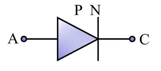
In the figure, the triangle on the left side represents the P-region of the diode, and the bar on the right side represents the N-region.
Working of PN Junction Diode
Now, let us discuss the working of the PN junction diode. When an external voltage is applied to a diode, then it is called the diode biasing.
There exist two types of biasing in a diode. These are-
- Forward Bias
- Reverse Bias
(1). Forward-Biased Diode
Forward biasing of the diode means joining the positive terminal of the battery to the P-type semiconductor material and the negative terminal of the battery to the N-type semiconductor material, as depicted in the following figure.
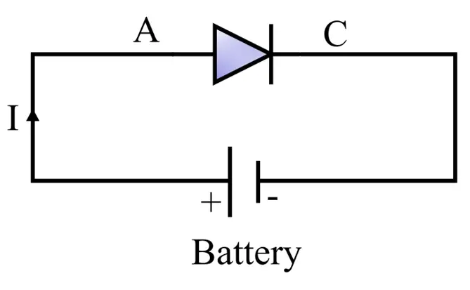
The applied external voltage to the junction diode reduces the potential barrier at the junction and allows current flow through it. When the diode is forward-biased, the majority charge carriers move toward the PN junction and create a substantial current flow. Due to the majority carriers, this current is termed forward current, and it increases with the increase in the forward bias voltage.
(2). Reverse-Biased Diode
Reverse biasing of a PN junction diode means connecting the battery’s positive terminal to the N-type semiconductor and the battery’s negative terminal to the P-type semiconductor, as shown in the following figure.
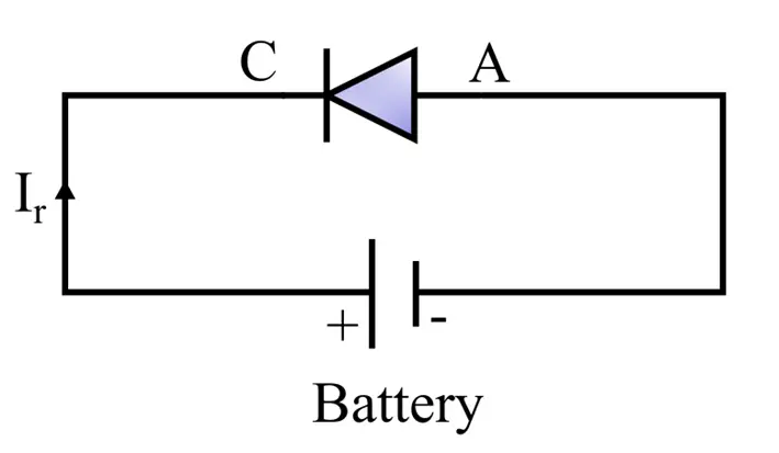
When the external voltage across a PN junction diode increases, the potential barrier increases and creates a reverse bias condition. The applied reverse-bias voltage creates an electric field that aligns with the potential barrier. As a result, the PN junction experiences a stronger electric field and increases the barrier width. This enlarged potential barrier effectively resists the flow of charge carriers across the PN junction. However, a very small current flows within the circuit due to the movement of the minority charge carrier, and this current is termed as reverse current or leakage current.
Hence, a forward-biased PN junction diode provides a very low resistance path, allowing current flow through the device. On the other hand, a reverse-biased junction diode provides a very high-resistance path to cease the current flow. Consequently, a PN junction diode can be used as a rectifier to convert alternating current into direct current.
Characteristics of PN Junction Diode
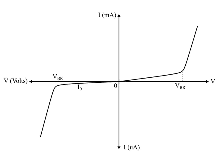
The performance of a PN junction diode can be analyzed through a graphical tool called VI characteristics.
The VI characteristics of a diode represent the relationship between the applied voltage across the diode terminals and the resulting current passing through it.
The performance of a diode can be analyzed in the following two distinct conditions:
- Characteristics during Forward Biasing
- Characteristics during Reverse Biasing
(1). Forward Characteristics Curve of a Junction Diode
The forward characteristics of a PN junction diode are shown in the following figure.
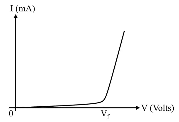
When the forward applied voltage to the diode is gradually increased, a knee voltage (Vf) is reached, which is 0.3 V for Ge and 0.7 V for Si. This forward knee voltage completely eliminates the potential barrier at the PN junction and starts a current flow through the junction. This knee voltage is also known as the threshold voltage (Vth) or cut-in voltage.
The graph clearly shows that a negligible forward current flows through the diode until the barrier voltage (Vb) is less than the cut-in voltage. After reaching the threshold value by the external voltage, a rapid exponential increase in the current is noticed through the diode. This segment of the curve is called the linear operational region of the diode.
It is also important to note that if the forward voltage exceeds a certain value, the diode may get damaged due to overheating.
(2). Reverse Characteristics Curve of a Junction Diode
When the PN junction diode is in the reverse biasing condition, it resists the flow of majority charge carriers and allows only a small current flow due to the minority charge carriers through the diode. When the reverse voltage increases from zero, the reverse current instantly attains its maximum limit, which is referred to as the reverse saturation current (I0) or leakage current.
The current flowing through the diode during the reverse-biased condition is plotted against the reverse voltage. The resultant graph represents the reverse VI characteristics of the diode.
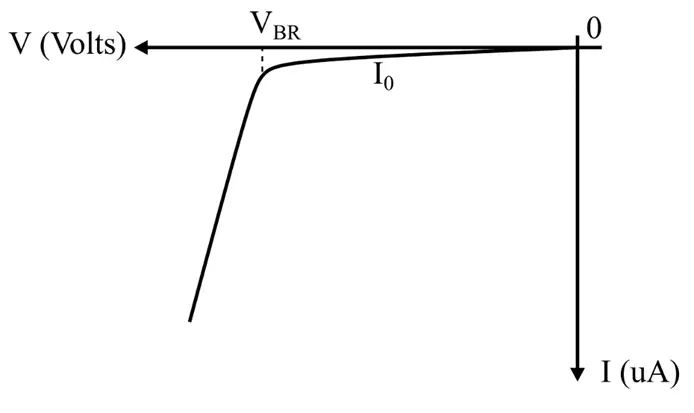
The graph demonstrates that when the applied reverse voltage remains below the reverse breakdown voltage (VBR), the current through the diode is very small and remains consistent. However, the leakage current increases abruptly once the reverse voltage crosses the breakdown voltage. At this point, the VI graph indicates zero resistance of the diode. In practice, the magnitude of the reverse current is of the order of microamperes (µA) for the Ge diode and nanamperes (nA) for the Si diode.
The further increase in the reverse voltage can damage the PN junction diode unless it is protected by a current-limiting resistor.
The combined VI characteristics of the diode are shown in the following figure.