Definition: The voltage at which the forward-biased diode starts conducting is called the knee voltage or cut-in voltage of the PN junction diode.
The Mechanism behind the Knee Voltage of a diode
The knee voltage in a pn junction diode is a result of the depletion region and barrier potential. These terms are further explained below.
Depletion Region:
The semiconductor diode is formed by bringing the n-type and p-type materials together. When the p- and n-type materials are joined, the electrons and holes in the region are combined, and a region is formed in which carriers are absent. This region of uncovered positive and negative ions is called the depletion region. The depletion region of the PN junction diode, when the diode is not biased, is shown below.
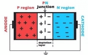
The width of the depletion layer reduces when the diode is forward-biased, and conversely, the width of the depletion layer increases when the diode is reverse-biased. The electric field is formed in the depletion region. For conduction of the diode, an external electric field needs to be applied across the diode to overcome the electric field formed in the depletion region.
Barrier Potential or Built-in Potential
The potential difference required to move the electrons through the electric field is called the barrier potential. The formula of the barrier potential or built-in voltage is given below.
Barrier Potential Formula
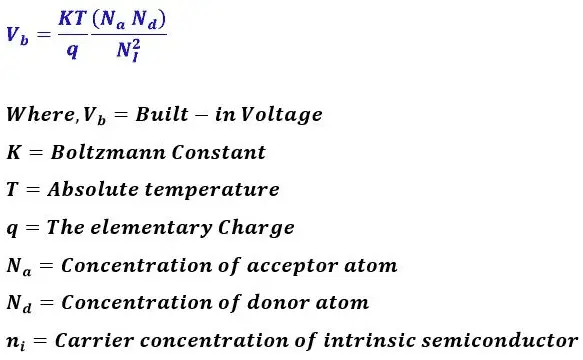
From the above, it is clear that barrier potential depends on the doping amount, temperature, carrier concentration of the undoped semiconductors, and the type of semiconductor material.
The concept explained above will help you understand the knee point voltage of a diode.
What is the knee voltage of the Diode?
The barrier potential or built-in potential is formed when the p- and n- junction is joined. If the diode is forward-biased when the battery’s positive terminal is connected to the anode and the negative terminal is connected to the cathode, the diode will not conduct unless the battery voltage exceeds the barrier potential.
The barrier potential of the germanium and silicon diodes are 0.3 and 0.7, respectively. For the silicon diode, if the battery voltage is more than 0.7, the diode starts conducting in a forward bias. If the applied voltage to the diode is less than the knee voltage, the diode does not conduct.
The minimum voltage at which the diode starts conducting heavily and the current starts increasing rapidly in a forwarding-biased state, the applied voltage, is called the knee voltage of the diode. The concept of knee voltage of the diode can be further understood with the help of forwarding characteristics of the diode.
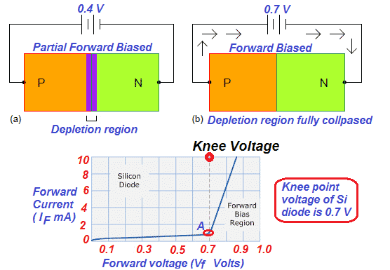
The diode is forward-biased by applying a positive and negative voltage at the anode and cathode of the diode, respectively. The applied voltage is increased gradually from zero voltage. The silicon diode does not conduct till the voltage reaches 0.7 volts. The germanium diode does not conduct till the voltage reaches 0.3 volts. The 0.7 and 0.3 volts are the knee voltage of the silicon and germanium diodes, respectively.
Once the forward voltage reaches the knee voltage, a small increase in voltage results in a large increase in current. This is due to the exponential relationship between current and voltage in a diode.
Numerical Problem on Knee Voltage of Diode
Now, we will further understand the knee voltage of a diode with the help of a numerical problem. We take the following circuit diagram.
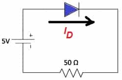
Calculate circuit current.
Knee Voltage of diode (Vk) = 0.7 V
Applied Voltage(V) = 5.0 V
Current limiting resistor(R) = 50 Ohms
Circuit Current (ID) = (V – Vk)/R
= (5 – 0.7)/50
= 4.3/50
ID = 0.086 A =86 mA
Conclusion:
In conclusion, the knee voltage of a PN-junction diode is a crucial parameter. It represents the minimum forward voltage required to overcome the built-in potential barrier of the depletion region. For silicon diodes, the knee voltage is 0.7 volts, while for germanium diodes, it is 0.3 volts.