In this article, we will discuss the operation of a bistable Multivibrator Using 555 Timer. A Bistable multivibrator has two stable states (high and low). It stays in the same state till the application of an external trigger input.
Before discussing on multivibrator, let us first discuss the internal configuration and design of IC555.
IC555 is an essential and integral component of an electronic circuit used for pulse generation, switching, and oscillator-based applications. The simple design and broader application base of this integrated circuit (IC) make it a popular addition to the dashboard of electronics hobbyists.
Design of an IC555 Integrated Circuit
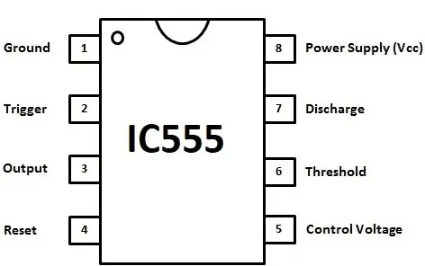
The above-given image is that of an IC555 integrated circuit. As evident, there are 8 pins in this circuit each with a distinct function. Let’s understand the function of each pin in brief. We will get more clarity on the working of these pins and the circuit as a whole in forthcoming sections when we will discuss the internal circuit of the IC as well as its application.
PIN 1 – Ground: As the name says, this pin is connected to the ground or the reference voltage.
PIN 2 – Trigger: A certain voltage is applied here externally such that it sends a high signal (trigger) whenever that voltage goes beyond a reference point ( discussed in detail in the later part of this post).
PIN 3 – Output: Generates output of the circuit as per the given input and connections made. This is the pin through which any switching application takes its input.
PIN 4 – Reset: An active low input pin is used to restart the IC.
PIN 5 – Control Voltage: Used to control the timing of the IC externally instead of how it does the same according to its internal circuit. In short, this pin allows customization of the IC555 as we want it to work.
PIN 6 – Threshold: Similar to Pin 2 (Trigger) except that this pin sends a high output when its voltage is above a certain set point. More clarity on this will come up in the later sections.
PIN 7 – Discharge: Used to discharge a capacitor employed for the purpose of timing control.
PIN 8 – Power Supply () – Connected to the voltage source or positive terminal of a battery.
Let’s understand the internal circuit of the IC to gain more clarity on what these pins exactly do. Only then we will be able to appreciate the utility of this IC.
Internal configuration of IC555
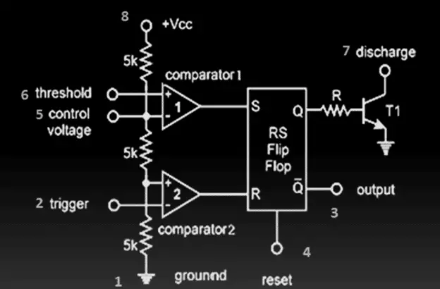
This is the internal circuit of the IC555 integrated chip. Pin 1 has to be connected to the ground and pin 8 to the Vcc. If you see the circuit clearly, you will find three 5k Ohm resistors being connected in series. This is the reason why the IC gets its name IC555.
There are two comparators or Operational Amplifier (OPAMP) followed by one SR FLIP-FLOP in the circuit. The negative or reference voltage pin of comparator 1 is connected to the leg connecting the three 5k Ohm resistors. Vcc has been applied at pin 8 and therefore by the voltage division method, we can calculate the voltage at the negative input of comparator 1 which is the reference voltage for the same.
This voltage is important because the comparator basically compares the two voltages at its ‘+’ and ‘-’ pin and sends a high output when the ‘+’ pin voltage is higher than that of the ‘-’ pin voltage. That means if we know the voltage at the first comparator’s reference or ‘-’ pin, we can set the threshold pin voltage accordingly to let the comparator send high or low output.
That’s why PIN 6 of the IC is called ‘threshold’ as when the voltage of this pin goes beyond a certain threshold which is nothing but the reference voltage of this comparator (comparator 1), it sends a high output to the SR Flip-Flop.
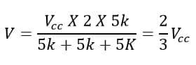
The reference voltage of comparator 1 (by voltage division method)
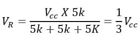
So, the first comparator sends a high output when its ‘+’ pin voltage (threshold pin voltage) goes above the threshold voltage of 1/3 Vcc.
PIN-5 of the IC is connected to the reference voltage of the comparator. This allows us to customize the reference voltage of the first comparator as per our requirements. This pin allows us to override the default reference voltage of 1/3 Vcc and gives us the control to change it externally as we want. That’s why PIN-5 is called CONTROL VOLTAGE PIN.
A similar analysis can be done in the case of the second comparator (comparator 2). Here the case is a bit different. Unlike the first comparator, here, the ‘+’ pin of the comparator has been connected to the leg of the three 5k Ohm series connected resistors while the ‘-’ pin of the comparator has been taken out as PIN 2 or TRIGGER pin of the IC.
That means, there will be a set voltage at the ‘+’ pin of the comparator and whenever the TRIGGER pin voltage will go below this set voltage of the ‘+’ pin, comparator 2 will send a high output (as the ‘+’ pin voltage automatically goes above the ‘-’ pin voltage of the comparator 2). That’s why PIN 2 of the IC is called TRIGGER as it controls the output status of comparator 2 by holding a trigger voltage externally which is nothing but a voltage below the ‘+’ pin voltage of the said comparator.
Here also, we can calculate this set voltage at the ‘+’ pin of the second comparator by using the voltage division method. This will be:
Thus if the TRIGGER pin voltage goes below 2/3 Vcc, comparator 2 sends a high output.
Finally, the outputs of both comparators go to an S-R Flip-Flop. The output of comparator 1 is connected to the SET pin (S) of the Flip-Flop while that of comparator 2 is connected to the RESET pin (R) of the Flip-Flop. The nature of the S-R Flip-Flop is that when the S pin is high, pin Q is high and the pin Q'(Q bar) becomes low (as it is the NOT operation of Q i.e, a NOT gate is internally connected which takes Q as input while Q'(Q bar) as the output). Again a NOT GATE is connected at the Q'(Q bar) which performs the NOT operation on Q'(Q bar) and gives the final output at the OUTPUT PIN (PIN 3 of the IC). When the RESET (R) pin of the Flip-Flop is HIGH, Q becomes LOW while Q'(Q bar) becomes HIGH and hence the final output at PIN 3 is LOW.
Now, let’s look at the entire picture. When the voltage at the THRESHOLD PIN (PIN 6) goes above the reference voltage of the first comparator, the S pin of the S-R Flip-Flop receives a HIGH input. As a result, Q becomes HIGH while Q'(Q bar) becomes LOW. As output at PIN 3 is the NOT operation of Q'(Q bar), the final output is HIGH.
Similarly, when the voltage at the TRIGGER pin (PIN 2) is lower than the voltage at the ‘+’ pin of the second comparator (i.e, 2/3 Vcc ), the second comparator sends a HIGH output. This causes the RESET (R) pin of the Flip-flop to become HIGH and consequently, the output at PIN 3 becomes LOW.
As you can see, the Q pin output is connected to the base of an NPN Bi-polar Transistor whose collector pin is known as the DISCHARGE PIN (PIN 7) of the IC. This DISCHARGE pin is connected to an external capacitor which is connected to the IC externally to control the timing of its output (i.e, by using an RC circuit). So, when the output from pin Q is HIGH, a positive voltage appears at the collector of the discharging transistor, and thus the added capacitor discharges through PIN 7 or the DISCHARGE pin to the ground. More clarity on this will come when we will discuss the application of this IC later.
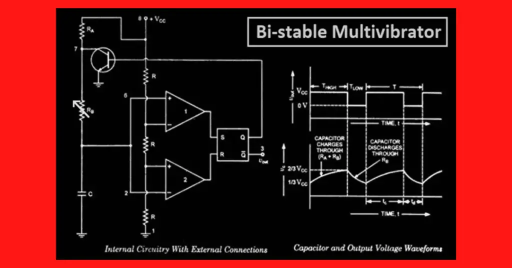
IC555 as Bi-stable Multivibrator
Operation of Bistable Multivibrator mode of 555 timer IC
The circuit diagram of Bi-stable multivibrator is shown below,
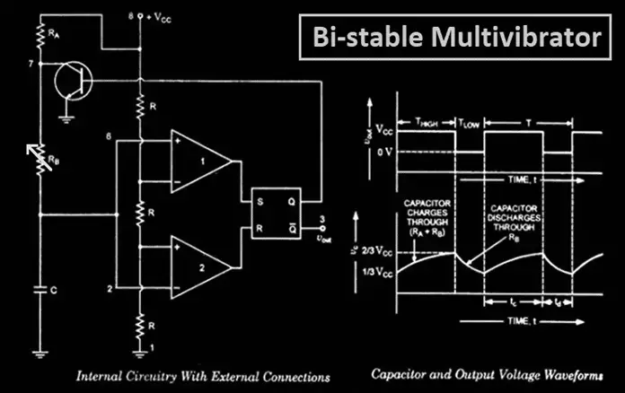
To operate the IC555 as a bi-stable multivibrator, we have to connect or short-circuit the THRESHOLD (PIN 6) and the TRIGGER (PIN 2). This is then connected to the external limb of the RC circuit as shown in the circuit diagram above.
At PIN 8, an appropriate voltage is applied. This causes the reference voltage of the first comparator to set at 1/3 Vcc while the voltage at the ‘+’ pin of the second comparator sets to 2/3 Vcc. At the same time, the externally connected capacitor begins to charge through the resistor RB. This capacitor voltage according to the circuit diagram, appears at the joint connection of PINs 2 and 6. Initially, the first comparator has a higher reference voltage and thus it remains in a cut-off state i.e, sends a LOW output to the SET pin of the S-R Flip-Flop. Thus, the output from pin Q of the Flip-Flop remains low while that of Q'(Q bar) remains HIGH. The output from comparator 2 is HIGH initially as the ‘+’ pin voltage remains higher than that of the ‘-’ pin voltage. This too results in the RESET input of the Flip-Flop remaining HIGH and hence the final OUTPUT from PIN 3 of the IC remains LOW.
The capacitor begins to charge through RB and its voltage reaches 2/3 Vcc. This voltage appears both at PIN 2 and 6 of the IC. Now, as soon as the capacitor charges further and its voltage goes above 2/3 Vcc, the positive input voltage of the first comparator becomes higher than the negative one and hence the output from the first comparator becomes HIGH. At the same time, the negative input voltage of the second comparator gains a higher voltage than that of its positive input and thus the output from the second comparator goes LOW. Both of these result in the SET of the Flip-Flop going HIGH while the RESET goes LOW. Hence the output from PIN 3 is HIGH as Q becomes HIGH while Q'(Q bar) becomes LOW.
Now, as Q goes HIGH, it causes the discharging transistor to activate as the Q pin is connected to the collector of that transistor. Thus, the charging capacitor now begins to discharge through RB and the transistor or PIN 7 (DISCHARGE PIN). As soon as the discharging capacitor voltage goes below 1/3 Vcc, the positive input voltage of the first comparator (PIN 6 of the IC) becomes lower than that of the negative input voltage and hence this comparator output is LOW while the second comparator gives a HIGH output as its negative input (PIN 2 of the IC) becomes lower than that of the positive input.
Thus the SET pin of the Flip-Flop goes LOW while RESET goes HIGH. Thus, the final OUTPUT from PIN 3 of the IC is LOW and at the same time, the output from pin Q of the Flip-Flop is LOW. This causes the discharging transistor to go into a cut-off state and hence the capacitor begins charging normally as it used to do before.
Again, the capacitor voltage goes above 2/3 Vcc and the same cycle repeats. Thus the capacitor keeps on charging and discharging between 1/3 Vcc and 2/3 Vcc respectively, thus causing the final output from PIN 3 of the IC555 to go LOW and HIGH respectively in a loop. This is what we call an oscillating output as shown on the right-hand side of the diagram above.
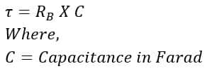
This application of the IC555 operates between two voltage levels, 1/3 Vcc and 2/3 Vcc and hence this is called Bi-stable Multivibrator. The oscillation frequency of the output from PIN 3 can be controlled using the variable resistor RB as it changes the time constant of the capacitor which is given by
This oscillating output from the IC555 can be used to drive a bi-polar junction transistor or IGBT or any other switching device controlling another circuit or application for example an inverter using the Pulse-width Modulation technique.
This shows the importance of IC555 as an integral component of switching or oscillation-based applications. By connecting external circuits, we can make use of this IC for various purposes likewise.