Insulated Gate Bipolar Transistor is a hybrid device. We call it IGBT in short. It is a something of a cross between the Bipolar junction Transistor(BJT) and Metal Oxide Semiconductor Field-effect Transistor(MOSFET). Thus, IGBT has the best characteristics of BJT and MOSFET.
The IGBT switches like MOSFET and conducts like BJT. Therefore, the switching and conduction behavior of the IGBT is excellent.
We also call IGBT as metal oxide insulated gate “transistor (MOSIGT), conductivity-modulated field-effect transistor (COMFET), or” gain-modulated FET (GEMFET). The initial name of IGBT was Insulated Gate Transistor (IGT).
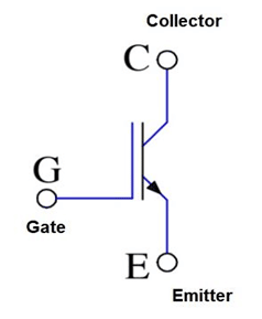
IGBT is a three-terminal device. It is one of the most important Power electronics devices.
IMPORTANT PROPERTIES
- We use it in low, medium, and high power appliances ranging from few voltages to thousands of voltages.
- The device offers excellent switching behavior
- For switching gate driver required is simple.
- provides a safe operating area and robust turn-off possibility.
- This device has a very good short circuit current limiting ability.
- This device conducts like a BJT and switches like a MOSFET.
- Switching speed is high and switching losses are low.
- This is a unidirectional device.
- I/P impedance is high.
- On-state voltage drop and power loss are lesser.
- Positive temperature coefficients for on state resistor therefore secondary breakdown will not occur.
Symbol of IGBT
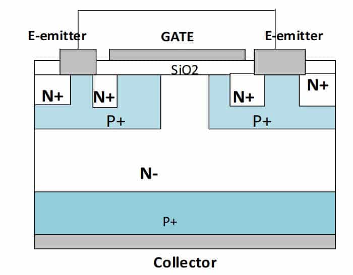
Construction of IGBT
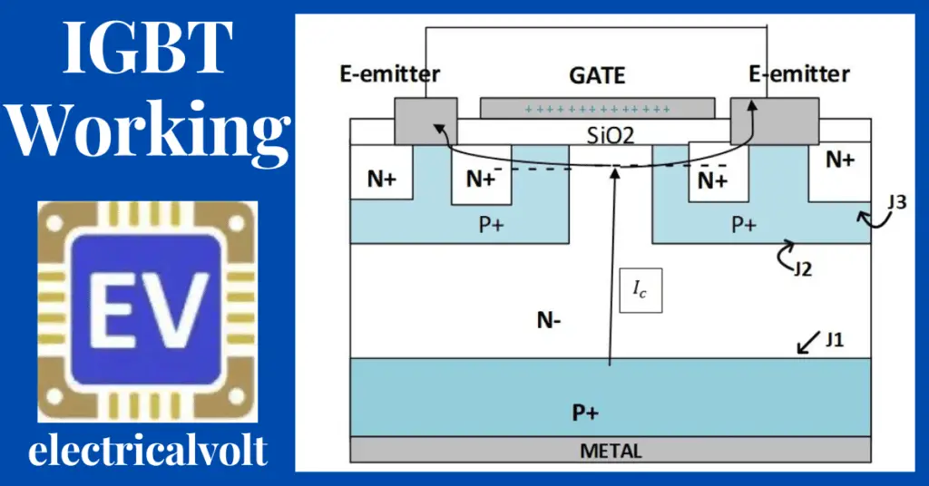
IGBT is a four-layer device, a four-layer of PNPN structure. The different terminals of an IGBT are shown in the figure below.
Equivalent Circuit Diagram
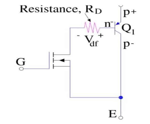
The approximate equivalent circuit of IGBT comprises MOSFET and PNP transistor. The resistance RD is the resistance of the n- region.
From the above figure, we can find out that as we move up we come across P+N-P layers. This means that IGBT is the combination of MOSFET and transistor. This is the basis for an approximate equivalent circuit. ‘You will notice that there exists ‘another path from collector to emitter; ‘this path is collector, p+, n–, p (n-channel),’ n+ and emitter. ‘There is, thus, another transistor Q2 as n–pn+ in the structure of IGBT. Thus, we need to incorporate this transistor Q2 in the approximate equivalent circuit to get the exact equivalent circuit.
Working Principle
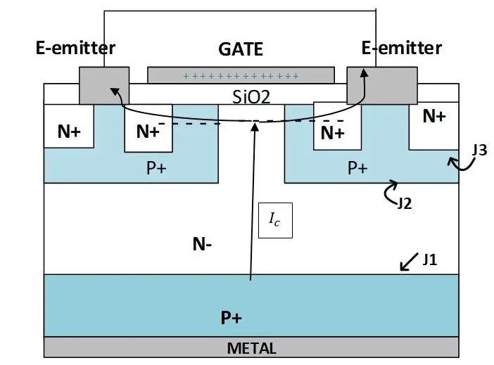
IGBT is a voltage-controlled device. The working principle of IGBT depends on the biasing of three terminals collector, emitter, and gate. When the collector is positive and the emitter is negative, the junction(J2) in reversed bias resists the flow of current.
On application of the gate signal at the gate terminal, it induces charges in the P+ region connecting the n+ region, and current flows from collector to emitter. The magnitude of the Gate voltage should be greater than the threshold (Vth). The channel so formed is called the inversion layer.
When the collector is positive and the emitter is negative, p+(collector) region injects holes into the n- , and at the same time, the emitter injects electrons into the n- layer. As a result, n- layer has enough charge carriers that increase the conductivity of the IGBT, and subsequently, IGBT gets on. So IGBT current is composed of both hole and electronics components.
The voltage drop in an IGBT during on state is very small so on state power loss is very low.
Applications of IGBT
The major application of IGBT is a power control switch because of its high voltage and current sustaining capabilities. IGBTs are most suitable as switching devices for motor drive systems, uninterruptible power supplies, induction cookers, and other applications. We widely use IGBTs as switching devices in the inverter circuit (for DC-to-AC conversion) for’ driving small to large motors. Also, IGBTs find wide applications for inverters used in home appliances such as air conditioners and refrigerators, industrial motors, and automotive main motor controllers to improve their efficiency.
Protection of IGBT
Electrostatic discharge of energy through the IGBT makes it more vulnerable to gate insulation damage.
With proper handling and application procedures, however, IGBTs are currently being extensively used in production by numerous equipment manufacturers in the military, industrial, and consumer applications, with virtually no damage problems due to electrostatic discharge
Precautions For Handling of IGBT
- Tips of soldering iron while soldering IGBT should be grounded.
- We must not remove the devices from the circuit when power is on.
- Gate voltage should be less than the rating of the voltage. Greater voltage than rated can permanently damage the oxide layer which acts as an insulator.
- Do not leave the gate open-circuited or floating. These conditions can result in “turn-on of the device due to voltage build upon the input capacitor due to leakage currents or pickup.”
- These devices do not have ‘an internal monolithic Zener Diode from gate to emitter. If gate protection is required an external’ Zener is recommended. ‘ECCOSORBD™ is a Trademark of Emerson and Cumming, Inc.’
- When “devices are removed by hand from their carriers, the hand being used should be grounded by any suitable means, for example, with a metallic wrist band..”
Gate Drive Circuit
The microcontroller generates the switching signals for IGBT. The output voltage of the microcontroller is generally 3-3.3 volts, which is not sufficient for IGBT triggering. If IGBT gets direct voltage from the controller, it may damage the high-cost controller due to insulation failure. That is why we use an amplifier to amplify the control signal to the suitable voltage with isolation between the power circuit and controller. The IC TLP250 (Toshiba make) is most suitable for gate drive switching purposes. PIN configuration and schematic diagram of TLP250 are given below.
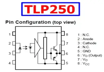
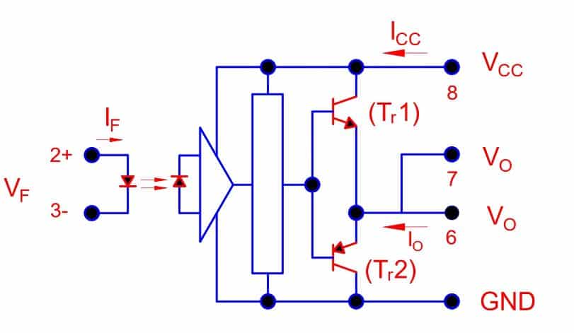
TOSHIBA TLP250 consists of a GaAlAs light emitting diode and an integrated photodetector which provides isolation. This unit is an 8−lead DIP package. This device is suitable for the gate driving circuits of IGBT or power MOSFET. Pin 6 or 7 is connected to the gate terminal of the IGBT.
Read Next: