This article describes IC 741 Op Amp basics. The operational amplifier (OP Amp) is a direct-coupled high gain amplifier. OP Amp usually consists of one or more differential amplifiers. It is usually followed by a level translator and an output stage. The output stage is a push-pull or a push-pull complementary-symmetry pair. The OP-AMP is available in the form of a single integrated circuit package.
OP-AMP can be used as a versatile device that can be used to amplify both dc and ac input signal. Initially, OP-AMP were used to perform mathematical operations like addition, subtraction, multiplication, and integration. By the addition of some external feedback components an OP-AMP can be used for many applications like ac or dc signal amplification, active filter, oscillators, comparators, regulators, etc.
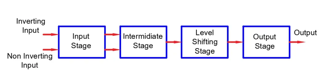
Block Diagram of OP AMP
OP-AMP is a multistage amplifier. The stages of an amplifier are:
1. Input Stage
This is the dual-input, balanced-output differential amplifier. In this stage, most of the voltage gain is provided. It also establishes the input resistance of an Op-amp.
2. Intermediate Stage:
In the intermediate stage, there is another differential amplifier that is driven by the output of the first stage. Generally, the intermediate stage is dual-input, unbalanced-output (single output). Due to the use of direct coupling, the dc voltage at the output of the intermediate stage is well above the ground potential.
3. Level Translator Stage:
A level translator (shifting) circuit is used after the intermediate stage so as to shift the dc level at the output of the intermediate stage downward to zero volt with respect to ground.
4. Output Stage:
Here in most of the cases, a push-pull complementary amplifier is used. The output voltage swing is increased and the current supplying capacity of the op-amp is also increased. If the output stage is well designed, it can also provide low output resistance.
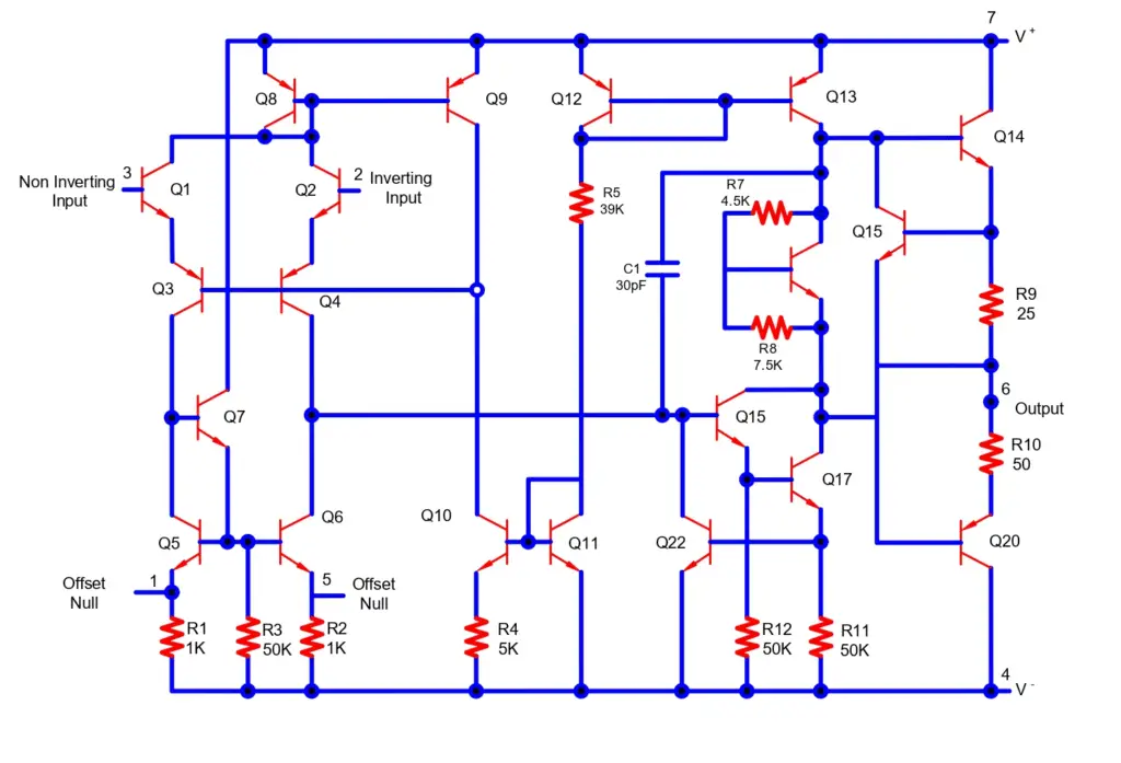
The internal circuit diagram of OP AMP is given below.
Schematic symbol of the OP-AMP
The schematic symbol of the OP-AMP is given below.
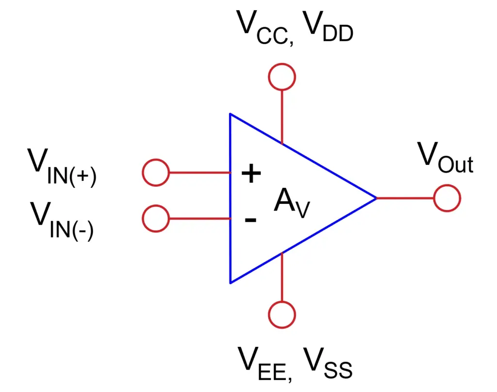
Where,
VIN(+): Non-inverting input
VIN(-): Inverting input
VOUT: Output
VCC, VDD : Positive Power Supply
VEE, VSS : Negative Power Supply
AV: Amplifier Gain
Inverting mode of OP-AMP
The input VIN(-) is the inverting input terminal. The ac signal or dc voltage applied to this input terminal produces a 180° out-of-phase (or opposite polarity) signal at the output.
Non-inverting mode of op-amp
The input VIN(+) is the non-inverting input terminal. Here, the ac signal or dc voltage applied to this input terminal produces an in-phase (or same polarity) signal at the output.
Integrated Circuits
Integrated circuits are devices have all the components of the circuit fabricated on a single chip. IC’s play a very important role in electronic circuit design. They are used in various fields like computer industry, automobile industry, home appliances, communication and control systems. By the use of IC’s miniaturization and superior performance are made possible. According to the mode of operation, IC’s are of two types: Digital or Linear.
The Digital IC’s have complete functioning network that are equivalent of basic transistor logic circuits. These are used in forming circuits like gates, counters, multiplexers, demultiplexers, etc.
They are predesigned packages so do not require anything other than power supply, input and output. They have two levels of voltage- high and low. The Linear IC’s are the equivalents of discrete transistor network, for example, amplifiers, filters, frequency multipliers, and modulators.
These often require additional external components for satisfactory performance. Say for an example, external resistors are required for controlling the voltage gain and frequency response of an op-amp. In the linear circuits, the output electrical signals vary proportional to the input signals applied or the physical quantities. Linear circuits are also called analog circuits.
OP-AMP IC’s are classified into two groups: general purpose and special purpose IC’s.
General-purpose OP-AMPs can be used in applications like integrator, differentiator, summing amplifier etc. One such widely used IC of OP-AMP is the 741 or 351.
Special purpose OP-AMP IC’s are used only in applications that they are specially designed for. For example, the LM380 OP-AMP can be used only for audio power applications.
Development of integrated circuits
Development of linear IC’s took place in the early 1960s, when arrays were first fabricated on single silicon chip. Arrays are the combination of isolated components such as diodes and transistors or individual stages such as differential amplifiers. Use of arrays helped in minimizing the temperature drift issue in discrete transistor and diode circuit. Because of arrays, the size of discrete electronic circuits also reduced significantly.
In 1963, Fairchild Semiconductor introduced the first IC op-amp, the mA702. This set to stage for development of another op-amp IC’s. The drawbacks of mA702 IC were: unequal supply voltages, such as +Vcc = +12V and –VEE = -6V, relatively low resistance(approx. 40kW), and low voltage gain( 3600V/V).
After this other generations of IC’s were designed and manufactured with updated technologies being incorporated. Some of the version are – mA709(by Fairchild in 1965. It is also regarded as first-generation OP-AMP), mA741 (second-generation OP-AMP). Other examples of second-generation OP-AMP are LM101, LM307, mA748, and MC1558.
IC 741
IC 741 is a monolithic OP-AMP IC. It is a general purpose operation amplifier. The number 741 indicates that the operational amplifier has 7 functional pins, 4 input pins, and an output pin. It has high voltage gain. They can be used in wide range of applications like integrators, summing amplifier and general feedback applications. The 741 also has short circuit protection and internal frequency compensation circuits built in it. IC 741 comes in the following form:
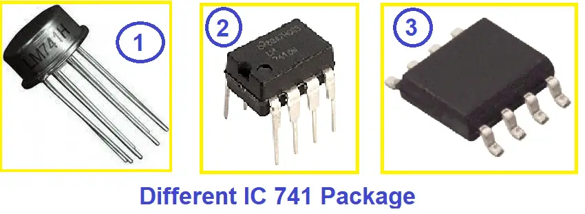
- Flat pack
- The metal can or transistor pack(TO5-8 Metal can package)
- The dual-in-line package (DIP)
- 8 Pin SOIC
Selection of IC Package
The selection of an IC package depends on the application.
If the IC is used in experimental or breadboarding purpose, the DIP package serves the best because of it is easy to mount. During mounting, it does not require bending or soldering of the leads. They are also suited for mounting in PCBs (printed circuit boards) because they have good led construction and good space between the leads. Ceramic DIP is expensive than the plastic DIP, but ceramic DIP dissipates more heat.
The flat pack IC is more reliable and lighter as compared to the DIP. It is therefore suited for airborne applications.
The metal can is best suited when the application is such that the IC is to be operated at relatively high power and is expected to dissipate considerable heat.
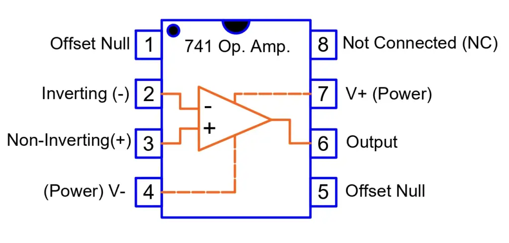
Pinout diagram of IC 741 Op Amp & their Functions
Pin Diagram of IC 741 in DIP-8 Package is shown in the below figure.
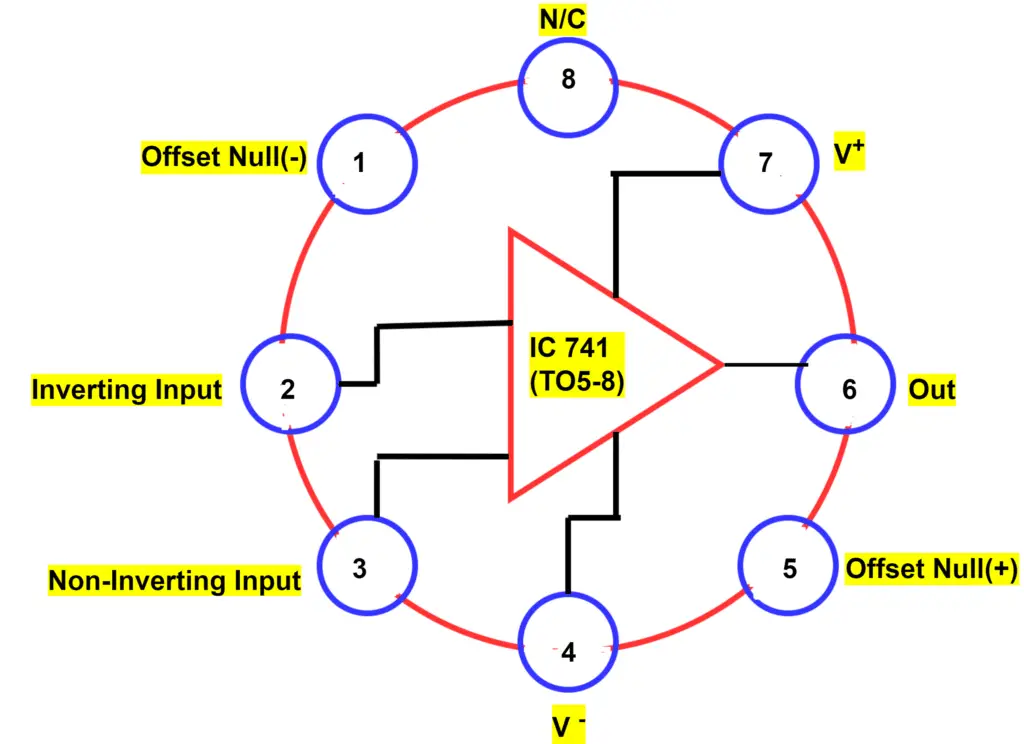
Pin Diagram of IC 741 in TO5-8 Package is shown in the below figure.
Pin Description of IC 741
The pin description of IC 741 is as follows.
Pin 4 & Pin 7: Power Supply
Pin 7 is the positive power supply terminal. Pin 4 is the negative power supply terminal. The voltage between these two pin will be between 5V and 18V. Usually the supply at +VCC is +15V and that at –VEe is -15V. These power supply voltages must be with referenced to a common point or ground.
Pin 6: Output Pin
The output from the op-amp is delivered to this pin. The voltage output received here depends on the feedback used and the voltage input given to the op-amp. When a high voltage is received at pin 6, it means the output voltage received is similar to the positive supply voltage. In the same way, if the output is said to be low, then the voltage at pin 6, corresponds to the negative supply voltage.
Pin 2 & Pin 3 : Input Pins
Pin2 is the inverting input of the op-amp. Pin 3 is the non-inverting input of the op-amp.
When the voltage at pin 2 is greater than the voltage at pin 3, it means that the inverting terminal has higher voltage. So, the output signal would be low.
When the voltage value at pin 3 is higher than the voltage at pin 2, the voltage level at non-inverting input is high. So, the output signal obtained would be high.
Pin 1 and Pin 5: Offset Null
Op-amp 741 provides high gain due to which minor differences in voltages at the inverting and non-inverting terminals can influence output. To nullify this influence, an offset voltage may be applied to the op-amp. This offset voltage is applied at pin 1 and pin5. It is usually done by using a potentiometer.
Pin 8: Not Connected
It is not connected to any part inside the IC 741. It is a dummy lead that is used to fill the void space in standard 8 pin packages.
Specifications of IC 741
- Power Supply: It requires minimum voltage level of 5V and can withstand till 18V
- Input Impedance: It is approx. 2MW
- Output Resistance: It is approx. 75W
- Voltage Gain: It is about 2,00,000 for low frequencies (200V/mV)
- Maximum Output Current: It is about 20mA.
- Recommended Output Load: It is greater than 2kW
- Input offset: It ranges between 2mV and 6mV
- Slew Rate: 0.5/ms
(Slew rate is the rate at which an OP-AMP can detect voltage changes in the input)
CHARACTERISTICS OF AN OP-AMP
| Characteristics | Ideal | Practical |
| CMRR | Infinite | 120 dB |
| Slew Rate | Infinite | 80 V/ms |
| Input Resistance | Infinite | 106 W |
| Output Resistance | Zero | 100 W |
| Gain | Infinite | 106 |
| Bandwidth | Infinite | 106 Hz |
| Offset Voltage | Zero | Negligible |
| Offset Current | Zero | Approx. In nA |
CMRR- Common Mode Rejection Ratio. It is ability of the differential amplifier to reject the portion of signal common to both the positive and negative inputs.
Applications of IC 741
The followings are the applications of IC 741 Op Amp.
- Amplifiers: 741 IC is widely used as an amplifier for DC to higher radio frequencies. It is also used for filtering the unwanted signals. Examples- tone control system in stereo and High Fidelity Systems.
- Computational: 741 IC is used for performing mathematical operations like integration, differentiation, summers etc.
- Rectifiers: IC 741 can function as an ideal diode and it does not cause voltage drop. An ordinary diodes used in rectifiers have voltage drop across them. Therefore, diodes are not suitable for high accuracy signal rectifiers.
- Oscillators: Op-Amp IC 741 is used to generate different output waveforms like sinusoidal, square, triangular etc. It is also used for PMW generator.
- Comparators: The 741 IC has functionality to work as a comparator. It compares voltage signals and outputs voltage according to magnitude of the incoming voltage. We can use IC 741 as a voltage regulators and signal comparators.
- ADCs / DACs: 741 Op-Amp is used for converting the digital signal into an analog signal.