This article describes two transistor model of SCR or Thyristor. A thyristor, also known as Silicon Controlled Rectifier (SCR) is a three-terminal power electronic device used in various electronic applications like rectifiers, SMPS, etc. as a switching device. It has three terminals – Anode, Cathode, and Gate.
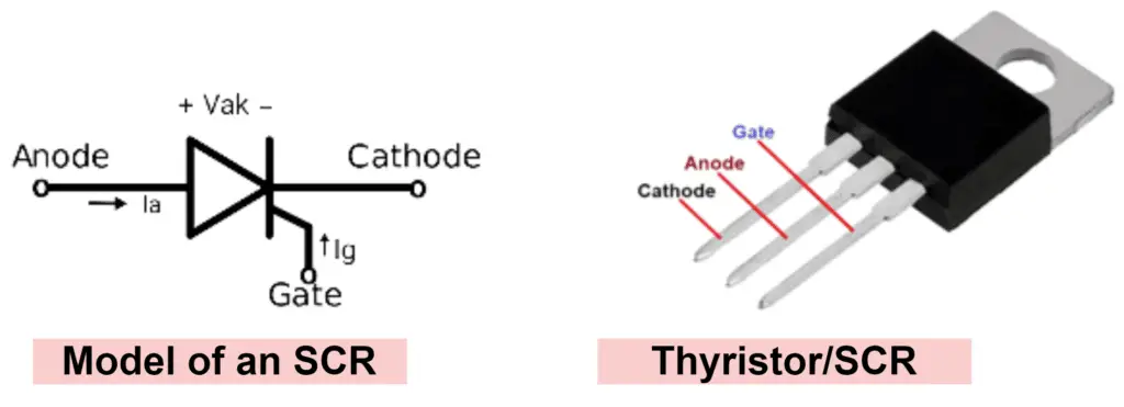
An SCR or Thyristor is similar to that a diode except for the fact that it has an additional control pin. Unlike a diode, an SCR needs positive voltage across the gate terminal as well in addition to the anode and cathode being connected to the positive and negative terminal of a voltage source respectively.
Thus, the output from an SCR can be controlled by simply controlling the gate voltage at an appropriate instant of time without having to connect and disconnect the supply. This gives an added advantage to the SCR over the diode in applications where voltage control is required.
For a rectifier using diodes, the output will be there for the complete positive half cycle and we can’t control it. But with SCR, we can decide when the gate voltage has to be applied and therefore we can give the gate pulse at that instant to get the desired output. This increases the efficiency of the entire system and allows smoother operations in the case of motor drive applications.
Two transistors model of SCR
Unlike other power electronic devices, an SCR needs a positive pulse across the gate terminal only once to activate. Once the gate current is equal to or above the latching current, the SCR activates and the gate voltage can be turned off. The SCR doesn’t need a constant voltage across the gate terminal. This is because of its two-transistor mode of working. Let us understand it in detail.
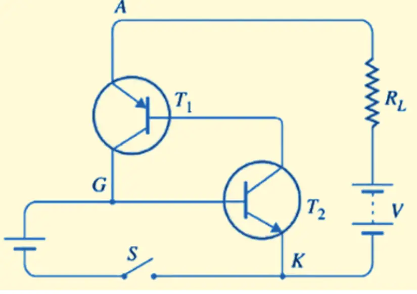
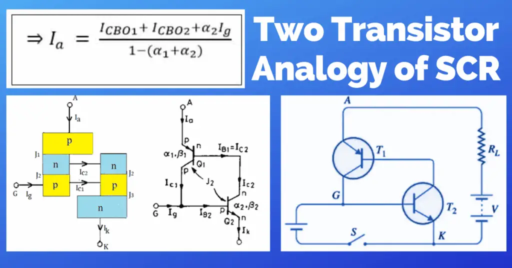
An SCR can be shown as two back-to-back connected bipolar junction transistors as shown above in the picture. Both the transistors are PNP and NPN type respectively. Here T1 denotes the PNP type while the NPN type transistor has been denoted by T2. The base terminal of the T1 transistor is connected to the collector terminal of the T2 transistor.
The collector terminal of the T1 transistor is connected to the base of the T2 transistor. This is the back-to-back connected transistor model of an SCR. The junction G in the image shown denotes the GATE terminal of this SCR while A and K denotes the ANODE and CATHODE terminals respectively.
It must be noted that for the NPN-type transistor to conduct, a positive voltage is required at the base whereas a PNP-type transistor conducts when there is a falling pulse or a negative voltage is applied at its base terminal.
Now, in the above-given circuit, switch S is closed at an appropriate instant time. This causes a positive pulse to appear at the base terminal of the transistor T2 and it starts conducting. Assuming there is no voltage drop between the collector and emitter of the transistor T2, we can say that it starts working like a short circuit. This causes the negative terminal voltage of the battery to appear at the base of the PNP transistor T1.
As an NPN transistor needs a negative voltage at its base to start conduction, the transistor T1 also starts conduction. Therefore both T1 and T2 behave as a short-circuited path (assuming negligible voltage drop) and thus a load current begins to flow from the supply V through the load represented by resistance R. This is what constitutes the two-transistor model of SCR or Thyristor.
Transistor latching in SCR
Latching of transistors in an SCR causes one transistor to drive the other one and therefore there is no need for any external base voltage supply in the case of the transistors or gate voltage supply in the case of the SCR. Let’s understand the latching process.
In the above-given model, the switch S when connected, causes a positive voltage to appear at the base terminal of the transistor T2. As a result, T2 starts conduction and the negative terminal voltage of the gate supply appears at the base terminal of the transistor T1. This causes the transistor T1 to begin conduction as well.
Now as T1 is conducting, it causes the positive voltage from the source ‘V’ to appear at node G (assuming a negligible voltage drop across T1). As the base of the NPN-type transistor T2 is in common with node G, this positive voltage appears at the base of the respective transistor. This causes the transistor T2 to continue conduction.
As T2 is conducting, it causes the negative terminal voltage of the source to appear at its collector. The collector of the transistor T2 is connected to the base of the PNP transistor T1. Thus the transistor T1 also keeps on conducting. In this way, both the transistors keep on running each other which is known as the latch mode of working. That’s why there is no role of the gate supply after turning on the latch process within an SCR.
Once latched, both the transistors connected back-to-back (representing an SCR) keeps on working and need no gate supply. This makes SCR a unique power electronic device where you need a gate supply only during the start and not for continued operation.
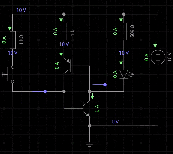
Here is an animation representing the two-transistor model of an SCR and its working. Notice how the push button connected to the gate terminal or the common base terminal is required only to start the conduction process. Once that happens, there is no control of the push button over the entire process.
This is exactly what happens in a Silicon Controlled Rectifier (SCR). To stop it from conducting, the current through the SCR has to be reduced below the latching current so that the latching of the transistors could be stopped.
Mathematical Analysis of the two-transistor model
The thyristor when bisected from the middle, has two parts – an NPN-type transistor and a PNP-type transistor connected back-to-back as we discussed above. The picture given below is that of a thyristor bisected from the middle.
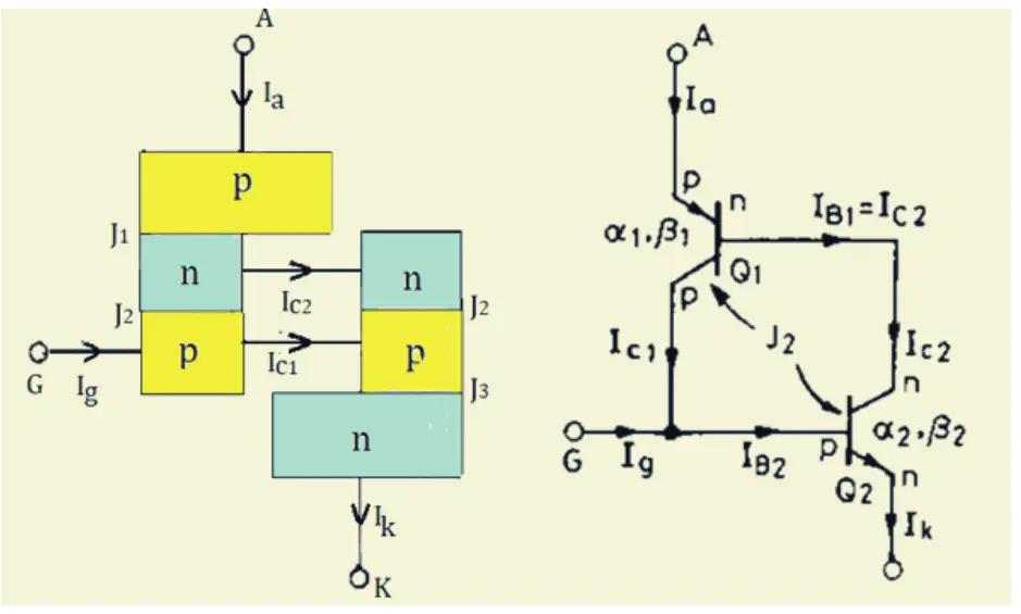
Terminal A denotes Anode, K is the cathode and G is the gate while Ia, Ig, and Ik denote the anode current, cathode current, and gate current respectively.
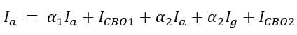
Now, according to the transistor leakage current equation, the collector current is given as
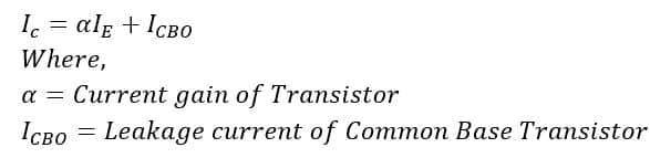
Therefore for the first transistor T1, we can say,
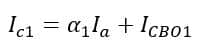
As for the first transistor, the emitter current equals to the anode current Ia.
For the second transistor, T2
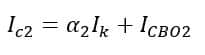
As the emitter current in the case of the second transistor is equal to the cathode current of the second transistor Ik.
By applying KCL in the circuit, we can say,
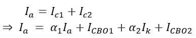
Again, by applying KCL, we can say
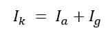
Therefore, Ia can be given as
Hence,
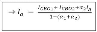
Therefore, it is clear that with the increasing value of ( α1 + α2), it approaches the value 1 (unity) and the anode current keeps on rising. This rise in the value of ( α1 + α2) is the result of a cumulative increase in the value α1 and α2 which begins with the supply of the gate current Ig in the beginning.
This buildup of α1 followed by α2 again followed by α1 keeps ongoing and the anode current rises. This buildup process is called the latching of the SCR or Thyristor. That’s why the gate current is required only to start the transistor’s latching process, which sets on as the anode current is equal to the latching current. This can also be seen in the characteristic curve of the SCR.
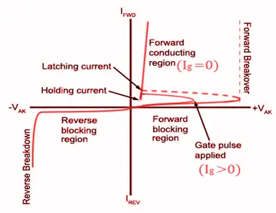
As you can see, the gate pulse (Ig) is applied at a certain instant causing the current to reach the latching current value. As the conduction begins in the forward conducting region, Ig is no longer required and hence it is equal to zero while the conduction goes on itself due to latching.
It is also clear from the characteristic curve that the latching current must be greater than the holding current for the forward conduction to begin.
The explanation I got for the working SRC was very extensive and helpful for me. I love all these concepts explained here. I wish I could reason and become like you people.