In this article, we shall learn about bipolar junction transistor (BJT), their definition, construction, types, and applications.
What is a Bipolar Junction Transistor?
A bipolar junction transistor, abbreviated as BJT, is a three-terminal semiconductor device that can function as a static switch or an amplifier. In practice, the BJT is also referred to as a transistor. The BJT was invented by W. Shockley, J Barden, and W. Brattain in the year 1947.
The name of BJT, i.e. transistor, is derived from two terms ‘transfer’ and ‘resistor’. It is because these two words can describe the operation of BJT, which is the transfer of a signal from a low-resistance circuit to a high-resistance circuit.
Why BJT is Called Bipolar?
A bipolar transistor is a three-terminal semiconductor device. It has two kinds of semiconductor materials P-type (positive type) and n-type (negative type), and the current flow through these regions. Therefore, it is called a bipolar transistor.
Construction of Bipolar Junction Transistor(BJT)
A bipolar junction transistor is constructed by sandwiching a p-type (or n-type) semiconductor between two layers of an n-type (or p-type) semiconductor as shown in figure (1). A metallic contact is attached to each of the three layers which act as the terminal of the transistor.
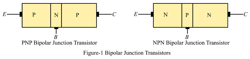
The three semiconductor layers of the bipolar junction transistor are named as emitter (E), base (B), and collector (C). The emitter is the region that emits the charge carriers, the base is the region that acts as the controller and collector is the region which collects the charge carriers. The emitter is a moderately sized and highly doped region, the base is the smallest and lightly doped region, and the collector is the largest in size and lightly doped region.
From figure (1), we can observe that the BJT has two pn-junctions namely the emitter-base junction and collector-base junction. Therefore, the BJT is a two-junction, three-terminal semiconductor device.
Terminals of BJT
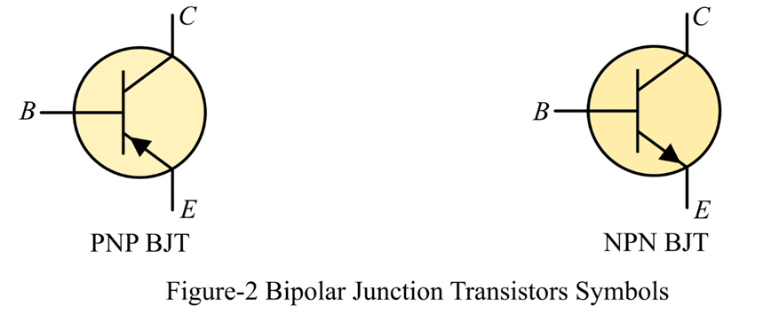
The BJT has three terminals, such as base, Emitter, and Collector. The emitter of a BJT has an arrow symbol and the direction of the arrow represents the current flow direction.
Emitter Terminal
The emitter terminal emits the charge carriers- holes in the PNP transistor and electrons in the NPN transistor. The emitter is the most heavily doped among all three terminals. The base terminal is always kept reverse-biased with respect to other terminals in order to produce huge majority carriers.
The emitter-base junction is forward-biased for PNP & NPN transistors. The emitter terminal provides electrons and holes toward the EB-junction in NPN and PNP transistors respectively.
Collector Terminal
The collector is the reverse side of the Emitter terminal and it collects the emitted charge carriers. Therefore, this terminal is heavily doped. The CB-junction is kept reversed-biased in both transistors.
The collector terminal of the transistor collects electrons emitted through the emitter terminal in the NPN transistor, whereas it gathers holes emitted through the emitter terminal in the PNP transistor.
Base Terminal
The base terminal is the middle part among collector & emitter terminals and forms two PN junctions among them. The base of the BJT is the most lightly doped segment. Therefore, the base controls the charge carriers flow from emitter & collector terminals.
Types of Bipolar Junction Transistor
Based on the construction, there are two types of BJT-
- NPN Bipolar Junction Transistor
- PNP Bipolar Junction Transistor
NPN Bipolar Junction Transistor
An NPN bipolar junction transistor is constructed by sandwiching a layer of p-type semiconductor between the two layers of n-type semiconductor. In the case of the NPN BJT, the two n-type semiconductor layers act as emitter and collector respectively. While the p-type semiconductor layer acts as a base. The structure and circuit symbol of an NPN BJT are shown in figures (1) and (2) respectively.
PNP Bipolar Junction Transistor
PNP bipolar junction transistor has a layer of n-type semiconductor sandwiched between the two layers of p-type semiconductor. In a PNP transistor, the two p-type semiconductor layers act as emitter and collector respectively, and the n-type semiconductor layer acts as the base of the transistor. The structure and circuit symbol of a PNP BJT are shown in figures (1) & (2) respectively.
Operation of Bipolar Junction Transistor
A BJT can operate in three regions namely active region, saturation region, and cut-off region. As we already discussed that a BJT consists of two PN-junctions namely the emitter-base (EB) junction and the collection-base (CB) junction.
Active Region
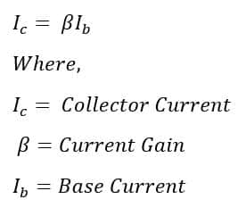
When one junction of BJT is forward-biased and the other is reverse-biased, then the BJT is said to be operated in the active region. In the active region, the bipolar junction transistor function as an amplifier. We get amplified collector current when a small base current flows. The current gain of the transistor is ‘β’.The magnitude of collector current can be expressed by the following mathematical expression.
We call the active region a linear region that lies between the cutoff & the saturation region of BJT. The amplification operation of this transistor occurs within this region.
Saturation Region
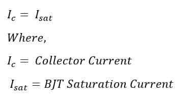
When both PN junctions of a bipolar junction transistor are forward-biased, in this case, the BJT is said to operate in the saturation region. The transistor operating in saturation region works as a closed switch and conducts electric current. In the saturation region, the highest current( Saturation current ‘Isat’) flows in the emitter and collector.
Cutoff Region
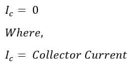
When both PN junctions are reverse-biased, the BJT is said to operate in the cut-off region and does not conduct current. Hence, a bipolar junction transistor in the cut-off region acts as an open switch. Cutoff region operation is contrary to the operation of BJT in the saturation region. In the saturation region, the collector current is the highest, whereas no collector current flows in the cutoff region. The cutoff region can be achieved when the voltage across the base to emitter junction is less than 0.7 volts.
The collector current in the cutoff region is zero.
Configuration of Bipolar Junction Transistors
The bipolar transistor can be connected in three configurations. They are,
- Common Emitter Configuration – This configuration has both voltage and current gain
- The common Collector Configuration – The configuration has no voltage gain but has a current gain
- Common base configuration – It has no current gain but has a voltage gain
The below table describes the Characteristics of different transistor configurations.
| Characteristics | Common Emitter | Common Collector | Common Base |
| Power Gain | Very high | Medium | Low |
| Current gain | Medium | High | Low |
| Voltage gain | Medium | Low | High |
| Phase angle | 180 | 0 | 0 |
| Output impedance | High | Low | Very High |
| Input Impedance | Medium | High | Low |
Applications of Bipolar Junction Transistor
The bipolar junction transistor is extensively used in a number of electronic devices and systems. The bipolar junction transistors are used as a switch, as an amplifier, as a filter, and as an oscillator. Below is the list of other applications of bipolar junction transistors: Some major applications are listed below:
- A bipolar junction transistor is used for signal amplification purposes.
- BJT is used as a solid-state switch.
- BJT is used to realize logic gates, etc.
- As a detector for demodulation of the modulated signal.
- For clamping circuits