In electrical engineering, input impedance defines how an electrical network resists the flow of current when viewed from the perspective of an external power source. This value encompasses both the static opposition known as resistance and the frequency-dependent dynamic opposition called reactance. Conversely, input admittance represents the inverse of this impedance, serving as a metric for how easily a load network accepts current from a source.
Within this framework, the source network is responsible for power transmission, while the load network acts as the consumer. When using diagnostic tools—such as an oscilloscope—to analyze a circuit, the instrument itself functions as the “load”. Therefore, the input impedance of an oscilloscope is essentially the electrical “burden” or characteristic impedance that the measurement device imposes on the circuit currently under observation.
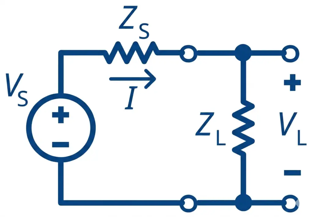
What is Input Impedance?
The interaction between source and load networks is a fundamental concept in electrical engineering, managed through the principle of equivalent circuits. When you substitute a load network with another device having the same input impedance, the behavior of the source-load system remains unchanged from the connection point’s perspective. This ensures that both the voltage across the input terminals and the current passing through them remain consistent with the original load.
Ultimately, the way voltage and current change within a network is determined by the specific relationship between the source’s output impedance and the load’s input impedance. This principle is essential to Thévenin’s theorem, which utilizes the concept of input impedance to calculate the equivalent impedance of a simplified electrical network.
In the circuit shown below, the network on the left side of the central open terminals represents the source circuit, while the network on the right side represents the connected load circuit. Here, ZS is the output impedance seen by the load, and ZL is the input impedance seen by the source.
High vs Low Input Impedance
The effect of input impedance on circuit performance can be better understood through the following comparison:
| Parameter | High Input Impedance | Low Input Impedance |
| Current Drawn | Very Low | High |
| Loading Effect | Minimal | Significant |
| Signal Quality | Better | Reduced |
| Typical Applications | Op-Amps, Oscilloscopes, FET Circuits | Power Circuits, Low-Resistance Loads |
Input Impedance Calculation
When dealing with electrical circuits, the behavior of signals is governed by the interaction between the source and the load. To understand how to calculate the transfer function—which describes how the input signal relates to the output signal—engineers use the equivalent circuit model.
By creating an equivalent circuit, you can simplify the math required to analyze the system:
- Source Representation: You represent the signal source in series with its output impedance.
- Load Representation: You represent the load network using its input impedance.
- Application of Ohm’s Law: With the circuit simplified into these two series components, you can use Ohm’s Law to determine the voltage division and current flow across the terminals.
Essentially, once the circuit is reduced to this basic series-load configuration, calculating the transfer function becomes a straightforward application of voltage divider rules derived directly from Ohm’s Law.
Example: Audio Preamp to Power Amplifier
Imagine you have an audio preamplifier (the source) connected to a power amplifier (the load).
- Source Representation: The preamplifier has an output voltage and an internal output impedance .
- Load Representation: The power amplifier has an input impedance (or ).
Calculation using the Voltage Divider Rule
In the circuit you provided, the output voltage (the voltage across the load) is determined by the voltage divider rule, which is a direct application of Ohm’s Law:
Plugging in our values:
Interpretation
The transfer function in this case is . This means that 99% of the source voltage is successfully transferred to the load. Because the input impedance of the load () is much higher than the output impedance of the source (), the signal is preserved with minimal loss, which is the goal in most practical circuit designs.
Electrical Efficiency and Impedance Bridging
Engineers evaluate the electrical efficiency of complex systems by segmenting them into individual stages. By analyzing the interaction between the output impedance (Zout) of one stage and the input impedance (Zin) of the next, they can determine the power transfer efficiency of the entire network.
Minimizing Signal Loss
To achieve maximum voltage transfer and minimize signal loss, the system must be designed so that the driving stage does not struggle to “push” the signal into the load.
- The Impedance Rule: Ideally, the output impedance of the signal source should be negligible compared to the input impedance of the connected network.
- Calculating Gain: The signal gain is determined by the ratio of the load’s input impedance to the total impedance of the circuit, which is the sum of input and output impedances.
- The Condition of Efficiency: For optimal performance, the following relationship must hold:
- Practical Implication: In this scenario, the input impedance of the driven stage (the load) is significantly higher than the output impedance of the driving stage. This configuration reduces power dissipation and helps preserve signal integrity.
To demonstrate how the impedance relationship minimizes signal loss, we use the voltage divider formula. This formula explains why keeping the input impedance (Zin) much higher than the output impedance (Zout) ensures that the majority of the source voltage is transferred to the load.
The voltage transfer is represented by the following ratio:
How this minimizes signal loss:
- Ideal Scenario (): When Zin is significantly larger than Zout, the term Zout becomes negligible in the denominator.
- Result: The expression simplifies to , which equals 1. This means nearly 100% of the signal voltage is successfully transferred to the load.
Input Impedance and Maximum Power Transfer
To optimize for maximum power transfer, a circuit must be designed so that the load impedance matches the complex conjugate of the source impedance. This process involves two key adjustments: the load resistance must equal the source resistance, and any system reactance must be neutralized to ensure the power factor is corrected.
When these conditions are met, the circuit is described as being complex conjugate matched to the signal’s impedance. The mathematical expression for this match is:
It is a common misconception that maximizing power transfer also maximizes electrical efficiency. In reality, when power transfer is optimized through this matching process, the system operates at only 50% efficiency.
- Reactive Components: The complex formula above is required when reactance is present.
- Simplified Condition: If the circuit contains no reactive components, the imaginary portion of Zout becomes zero. In this specific case, the condition simplifies to a basic resistive match,
Impedance Matching in Transmission Lines
When the characteristic impedance of a transmission line (Zline) differs from the input impedance of the connected load (Zin), the load network fails to absorb the full signal, causing a portion of the source energy to reflect back toward the source. This phenomenon often leads to the formation of standing waves along the transmission line.
To eliminate these reflections and ensure optimal signal delivery, the characteristic impedance of the transmission line must be equal to the load’s input impedance. This state is referred to as a matched connection, and the technique used to correct any existing mismatch is known as impedance matching.
Key Characteristics
- Geometry-Dependent: For a homogeneous transmission line, Zline is determined entirely by its physical geometry, making it a constant value.
- Consistency: Because the load impedance (Zin) can be measured independently of the line, the requirement for a matched connection remains valid regardless of where the load is positioned relative to the transmission line.
The fundamental condition for a perfect match is expressed as:
In practice, engineers use the Reflection Coefficient ( Γ) to measure how well the impedances are matched. It is defined by the formula:
- If : The reflection coefficient Γ = 0. No energy is reflected; this is a perfectly matched connection.
- If : Some energy is reflected, and the value of Γ indicates the severity of the mismatch.
Applications of Input Impedance
Signal processing
In modern signal processing, designers utilize impedance bridging to ensure high-fidelity signal transmission. This technique involves designing devices, such as operational amplifiers (op-amps), with an input impedance (Zin) that is several orders of magnitude higher than the output impedance (Zout) of the source.
Benefits of Impedance Bridging
- Minimal Signal Degradation: By maintaining , the amplifier draws negligible current from the source. Consequently, the input voltage remains nearly identical to the open-circuit voltage of the source, preventing loading effects.
- Buffering Techniques: If a component threatens to degrade the signal, engineers deploy intermediate devices—such as voltage followers or impedance-matching transformers—to act as high-impedance buffers, effectively isolating the source from the load.
Characteristics of High-Impedance Amplifiers
Devices like vacuum tubes, field-effect transistors (FETs), and op-amps are often modeled by a resistance in parallel with a capacitance (e.g., ). While these designs are essential for preserving signal voltage, they present specific trade-offs:
- Noise Considerations: High-impedance pre-amplifiers may exhibit a slightly higher effective input noise voltage. However, they provide a very low effective noise current.
- Noise Immunity: Systems configured with a relatively low-impedance source are generally more resilient to environmental interference, such as mains hum ( noise).
Impedance Mismatch in RF Power Systems
In Radio Frequency (RF) systems, maintaining impedance equilibrium is critical. When the transmission line and the load (such as an antenna system) are not properly matched, signal energy reflects back toward the source. This mismatch produces adverse effects that vary depending on the application:
- Analog Video: Mismatches manifest as “ghosting,” where a time-delayed echo of the signal creates a secondary, displaced image.
- High-Speed Digital Systems: Reflections introduce interference that can corrupt data, a significant issue in high-definition (HD) signal transmission.
The Danger of Standing Waves
Impedance mismatches create standing waves along the transmission line. These waves consist of periodic regions where the voltage is significantly higher than the intended operating levels.
- Dielectric Breakdown: If the standing wave voltage exceeds the dielectric strength of the line’s insulation, an electric arc can form.
- Component Damage: An arc can trigger a high-voltage reactive pulse, potentially destroying the transmitter’s final output stage.
RF Power Matching Standards
To prevent these issues, RF systems typically utilize standardized line and termination impedances, most commonly 50 Ω and 75 Ω. The standard serves as a critical engineering compromise:
- Power Handling: Higher impedances (near ) allow for greater power handling, but require cables with larger physical dimensions.
- Signal Loss (Attenuation): Lower impedances (near ) provide lower signal attenuation, but are less efficient for overall power transmission given common coaxial geometries.
- The Optimal Balance: The value was historically selected as the optimal equilibrium between these two competing factors for coaxial cable performance.
To maximize power delivery throughout the entire power chain—from the transmitter output, through the transmission line (coaxial cable, waveguide, or balanced pair), to the antenna—the circuit must be complex conjugate matched. This ensures the antenna system, which includes the impedance matching device and the radiating element, efficiently handles the power without generating harmful reflections.
Conclusion:
Input impedance is a key circuit parameter that influences voltage transfer, power transfer, signal integrity, and overall system performance. A proper understanding of the relationship between input and output impedance helps engineers minimize signal loss and optimize circuit operation. In practical applications, high input impedance reduces loading effects, while impedance matching is essential in RF and transmission-line systems to prevent reflections and maximize power transfer.
Read Next: