The voltage doubler produces two times DC voltage of the input AC peak voltage. This article describes the voltage doubler, its circuit diagram, types, working, advantages, and applications.
What is a Voltage Doubler?
An electronic circuit that generates an output voltage equal to double the input voltage is called a voltage doubler. It is also known as a voltage multiplier, as it multiplies the input voltage with a multiplication factor equal to 2.
It is important to note that we can increase the level of voltage by using a step-up transformer, however, the transformers are heavier and costlier devices. Therefore, for small electronic circuits and low-cost applications, a voltage-doubling circuit is used to increase the voltage level. A voltage doubler can increase the input voltage by a multiplication factor of 2 by using small electronic components like diodes and capacitors.
Types of Voltage Doubler
Voltage doublers are classified into the following two main types namely,
- Half Wave voltage doubler
- Full Wave voltage doubler
Let us discuss each type of doubler circuit in detail along with the construction and circuit diagram.
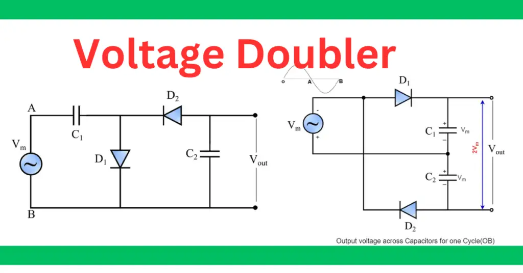
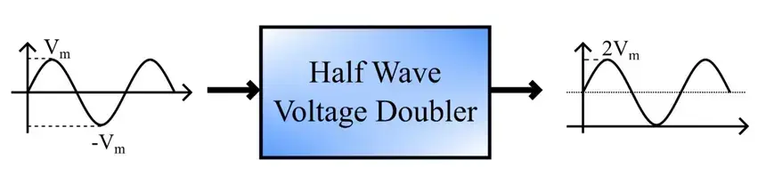
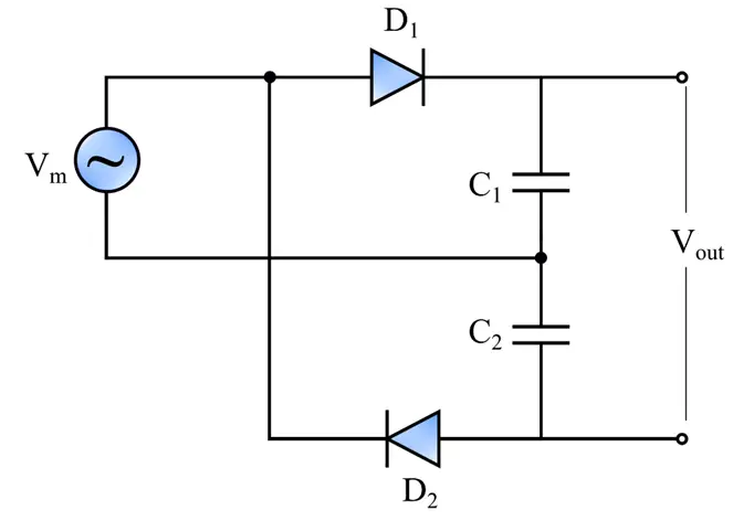
Half Wave Voltage Doubler
A half-wave voltage doubler circuit diagram is shown in the following figure.
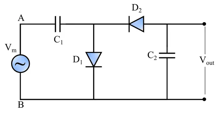
It consists of two pn-junction diodes and two capacitors that operate together to produce a double voltage of the input voltage.
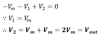
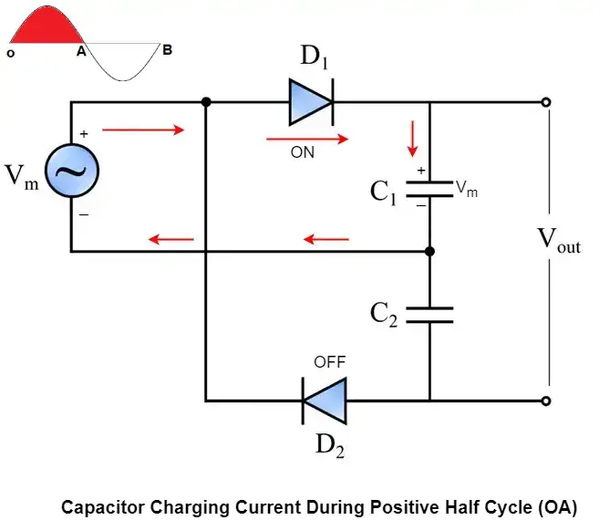
During the positive half-cycle of the input ac voltage, terminal A is at positive potential. In this period, the diode D1 conducts and charges the capacitor C1 to the maximum value of the input ac voltage Vm.
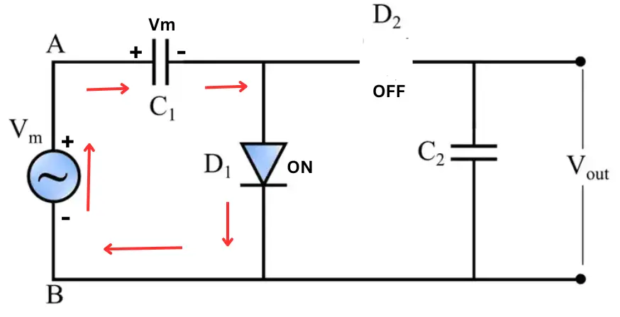
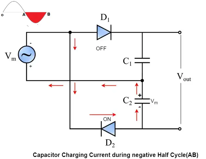
The capacitor C1 cannot release its energy due to the unavailability of a path because diode D2 is in reverse bias and hence remains in the fully charged state.
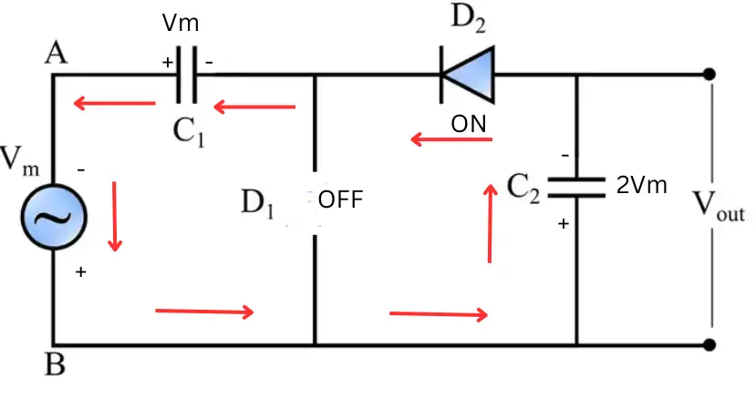
Next, during the negative half cycle, terminal B is positive and diode D2 starts conducting and diode D1 turned off due to the reverse bias state. Thus, the diode D1 being non-conducting stops the discharging of the capacitor C1, meanwhile, the diode D2 conducts and charges the capacitor C2 to a peak voltage 2Vm.
If V1 and V2 are the voltages across the capacitors C1 and C2 respectively, by applying KVL in the loop of the voltage doubling circuit, we get,
In the case of a half-wave voltage doubler circuit, the output voltage increases slowly. Another factor is that simply one-half cycle charges the capacitor C2. The output voltage has a ripple frequency equivalent to the supply frequency because a one-half cycle charges the capacitor C2.
The input and output waveform of the half-wave doubler circuit is shown in the below picture.
(2). Full Wave Voltage Doubler
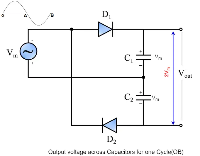
A full wave doubler circuit diagram is shown in the following figure.
Like the half-wave doubler, it also consists of two diodes and two capacitors, but the circuit’s configuration differs.
During the positive half cycle of input ac voltage, the diode D1 conducts and charges the capacitor C1 to the maximum voltage Vm.
During the negative half cycle of the input ac voltage, the diode D2 will conduct and charges the capacitor C2 to the maximum voltage Vm. During this period, the diode D1 will be in non-conducting mode.
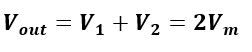
Since the two capacitors are connected in series, hence the output voltage will be equal to the sum of the voltages across the two capacitors.
Therefore,
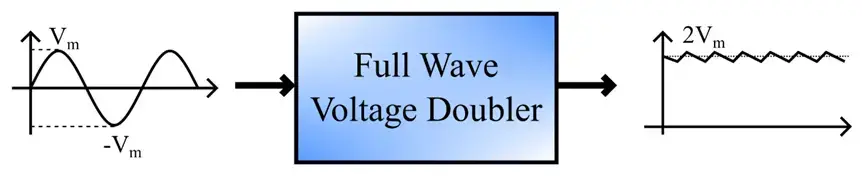
The input and output waveform of the full wave doubler circuit is shown in the below figure.
Advantages
A voltage doubler circuit has several advantages over a step-up transformer. Some key advantages are listed here:
- Light in weight and can replace heavy transformers
- Less expensive.
- More energy efficient due to the use of solid-state diodes.
- Easily scaled to higher order voltage multipliers simply by cascading more stages of voltage multiplication
Disadvantages
Apart from the advantages, voltage doublers also have some disadvantages. Some major disadvantages of voltage doublers are listed below:
- It Contains unwanted fluctuation, known as ripples
- Poor voltage regulation.
- Its output voltage depends upon the charge stored in the capacitors.
- It requires additional filter circuits to smooth the output voltage.
Applications of Voltage Doubler
The following are some important applications.
- Used in cathode ray tube televisions.
- Used in photocopier machines.
- They are also used in radar machines and X-rays machine.
- Also used in ion pumps and traveling wave tubes.
Hence, this is all about voltage doubler, their types, advantages, disadvantages, and applications.