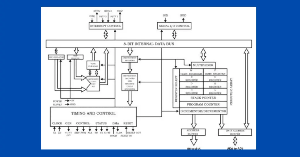
This article describes 8085 Microprocessor Architecture Diagram. Usually, the 8085 is an 8-bit microprocessor. It was launched by Intel in 1976 with the help of NMOS technology. The 8085 microprocessor is the updated version of the 4004 microprocessor. 8085 microprocessors have applications in microwave ovens, washing machines, gadgets, etc. The 8085 microprocessor is a 40-pin IC package that is fabricated on a single chip.
Configuration of 8085 Microprocessor Architecture Diagram
The 8085 Microprocessor Architecture Diagram has the following configuration:
- 8-bit data bus
- 16-bit address bus
- 16-bit program counter (PC)
- 16-bit stack pointer
- 8-bit registers
- +5V voltage supply
- 8085 microprocessor is operational on a 3.2 MHz single-segment CLK
8085 microprocessor has six 8-bit registers arranged in pairs- BC, DE, HL
Explain 8085 Architecture Diagram
The architecture of the 8085 Architecture Diagram gives information about what are the operations that can be executed and how these are performed.
The 8085 microprocessor can perform the below-given functions:
- Operate and store 8-bit data
- Execute arithmetic and logic operations.
- 8085 microprocessor can also sequence the instructions that are to be executed.
- 8085 microprocessor can store data on a temporary basis.
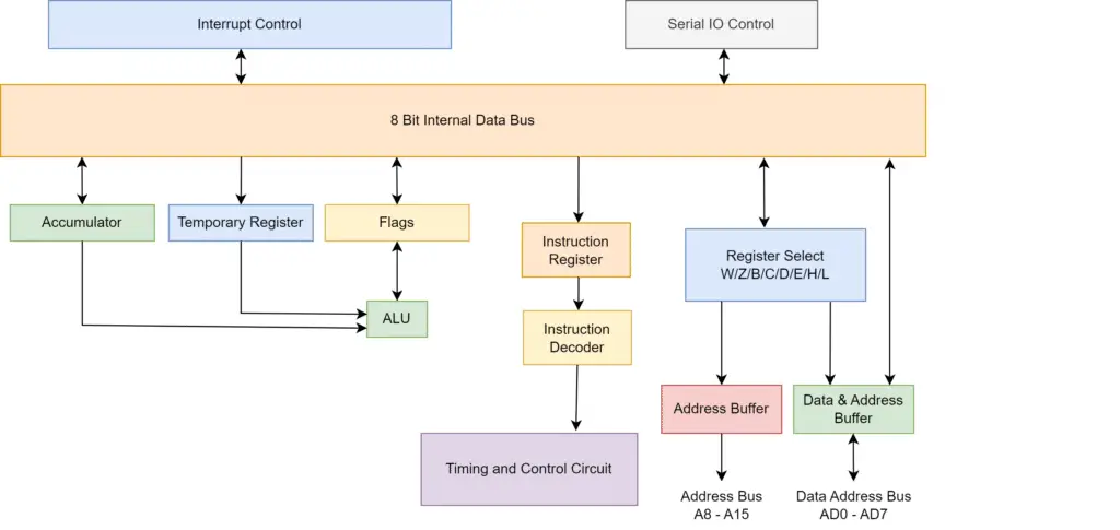
To perform all these operations, the processor of the 8085 microcontroller needs a control unit, arithmetic logic unit, registers, buses, etc.
Arithmetic logic unit
Arithmetic Logic Unit is abbreviated as ALU. ALU performs the arithmetic and logic operations on 8- bit data. Some operations are addition, subtraction, logical AND, logical OR, logical Exclusive OR, Complement (Logical NOT), Increment (add 1), Decrement (subtract 1), Left shift, Right shift, Rotate right, Rotate left, Clear, etc.
Functional Units of 8 Bit Microprocessor Architecture
The functional units of the 8 Bit Microprocessor Architecture are as follows:
Accumulator
The accumulator is also known as register A and is the heart of the microprocessor. It is an 8-bit register. An accumulator stores the result of an operation performed by the ALU. This is also connected to the internal data bus and ALU.
Registers
Registers are a set of flip-flops. They are used to hold/store data. There are two types of registers:
- General purpose registers: 8085 Microprocessor have 6 general purpose registers inside the microprocessor. General purpose registers store 8-bit data to execute a program. General purpose registers are named B, C, D, E, H, and L. General purpose registers are present in the microprocessor in the form of pairs- BC, DE, and HL. General purpose registers can be used to execute 16-bit operations also. General purpose registers are programmable registers which means, the programmer can access the general purpose registers to insert, transfer or delete data by using instructions.
- Temporary registers: The temporary registers are used by ALU for storing data temporarily. The programmer cannot access temporary registers. Temporary registers are of two types:
- Temporary data register: Temporary data registers hold the operand and then provide it to the ALU for the execution of the program. The immediate results will also be stored by ALU in this register. The temporary data register is an 8-bit register.
- W and Z register: W and Z registers are the registers that are also used for storing temporary data. W and Z registers are used by the control section of the microprocessor to store data during operations.
Program Counter (PC)
The program counter is a special-purpose register. The program counter is used to store the memory location of the instruction which is to be performed. This is because to fetch an instruction from the memory the microprocessor needs to know the address of the instruction. The program counter is a 16-bit register that stores addresses. It is used by the microprocessor to line up the instructions to be executed in a sequential manner. The program counter fetches the opcode from a memory location and simultaneously gets incremented by the next memory location.
Stack Pointer (SP)
The stack pointer is a 16-bit register. It is a part of the memory. When the data is stored in the stack it is in serial format. The stack pointer generally stores addresses of the last data element that is stored. So it is based on the Last Input First Output (LIFO). When new data is entered into the stack, the SP points toward the next memory location. When a data element is deleted, the SP will point to the previously occupied memory location.
Flags
The flag register is an 8-bit register. Flags hold the status of the current result which is generated by ALU. Flags do not have the current result of the operation. Hence, flags can be used to test data conditions.
The 8085 microprocessor has 5 flags. Flags show 5 different data conditions. Flags are-
- Carry (C)
- Sign (S)
- Zero (Z)
- Parity (P)
- Auxiliary carry flags (AC)
The bit position is as shown below:

Instruction 8 Bit Microprocessor Architecture register and decoder
The instruction register is an 8 Bit Microprocessor Architecture register. When an instruction is fetched, it is stored in the instruction register. The instruction decoder will decode the information contained in the instruction register.
Timing and Control unit (CU)
The timing and control unit is a part of the CPU. It performs the following functions:
- The timing and control unit generates the timing and control signals that are necessary for the execution of instructions.
- The timing and control unit controls the flow of data between the CPU and the peripherals, including memory.
- The timing and control unit provides status, control, and timing signals that are necessary for the operation of memory and I/O devices.
- The timing and control unit controls the entire operation of the microprocessor and the peripherals that are connected to it.
The timing and control unit provides the following signals that control internal and external circuits:
- Control Signals: READY, RD’, WR’, ALE
- Status Signals: S0, S1, IO/M’
- DMA Signals: HOLD, HLDA
- RESET Signals: RESET IN, RESET OUT
Interrupt control
The interrupt control always controls the interrupts during a process. During the execution of the main program, when an interrupt occurs, the microprocessor shifts the control from the main program to process an incoming request. After completion of the request, the control will go back to the main program. The 5 interrupt signals the 8085 Microprocessor has are: INTR, RST 7.5, RST 6.5, RST 5.5, and TRAP.
Serial input/output
The serial data communication is controlled using the instructions: SID (Serial Input Data) and SOD (Serial Output Data).
Address buffer and Address Data Buffer
The data in the stack pointer and program counter is loaded into the address buffer and address-data buffer to communicate with the CPU. The memory and I/O chips will also b connected to these buses. Hence, the CPU is able to exchange desired data with memory and I/O chips.
Address bus and data bus
The data bus will carry the data that needs to be stored. The data bus is bidirectional. The address bus carries the location where the data is to be stored. It is an unidirectional bus. The address bus is used to transfer data and address I/O devices.
Working of 8085 microcontroller
The function of a microcontroller is to execute instructions. So, in order to execute instructions, firstly, the instruction needs to be fetched, then decoded, and then executed. To fetch an instruction, the address of the instruction must be known. This is present in the program counter.
This fetched address is placed on the 16-bit address bus. It is then forwarded to the memory. Now, from the memory, the instruction is fetched from that particular memory location by the 8-bit data bus. At a particular time, the processor can only access either the data bus or the address bus. When the instruction is fetched from memory, through the internal buses, then the instruction is provided to the instruction register.
Now, the fetching of instructions from the memory is completed. The processor will now decode the instruction. This is then directly fed to the instruction decoder. The data and instruction in memory are stored in form of an opcode. The fetched opcode is analyzed by the instruction decoder present in the processor for executing the instruction. After fetching the instruction, the PC increments itself and thus provides the address location of the next instruction. The PC does not have any role in decoding and executing.
After the first instruction is executed, the next instruction is fetched from the memory. The timing and control circuit sends the control signals to various units of the microprocessor for the execution of instructions.
After execution of the instruction, the result is fed to the accumulator by the data bus. A flag register will hold the status of the result in the accumulator. After each instruction is performed by the ALU, the status of the flag register is changed. Hence, ALU will produce the result and the status simultaneously after each operation. The W and Z are temporary registers that the programmer cannot access. They are used by the processor to hold a temporary value that it stores.