Single Phase Semi Converter converts AC voltage into DC voltage in a controlled manner. We also call this a half-controlled converter. A single-phase semi-converter has two SCRs and two diodes. As its name suggests, the semiconductor has semi or limited control over the DC output voltage.
In this article, we will discuss in detail the single-phase semi-converter, its working, operation, average & RMS output voltage.
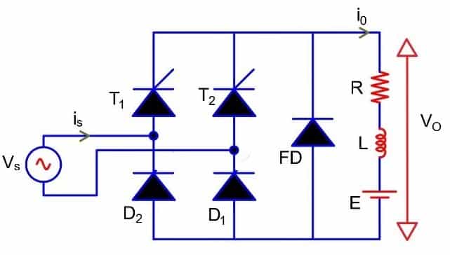
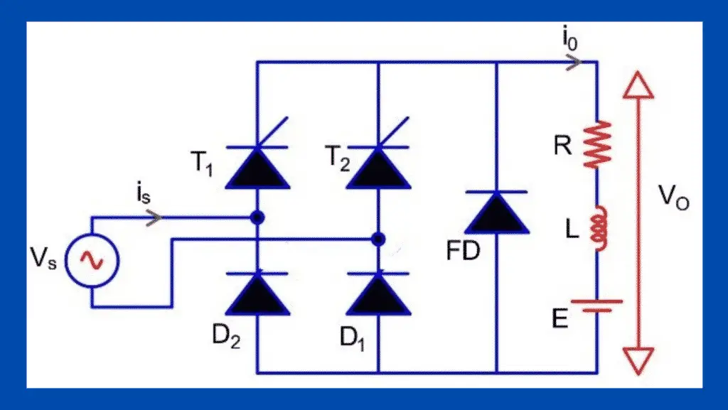
Circuit Diagram of Single Phase Semi Converter
The figure below shows the circuit diagram of single-phase semi-converter bridge circuit.
Working of Single Phase Semi Converter
The bridge circuit of the semi converter has two diodes (D1, D2) and two SCRs(T1, T2). Pair of a diode and SCR( D2, T1) is connected in the parallel with another pair of a diode and SCR(D1, T2). And, finally, the bridge circuit has a parallel connection with the RL circuit. Thus, this bridge circuit is the main circuit of the semi converter.
A free-wheeling diode (FD) has its connection in parallel with the load and bridge circuit. The freewheeling diode freewheels the energy stored in the inductor and, thus limits the overvoltage.
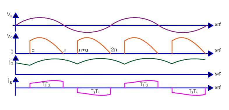
Waveform of Single-Phase Semi Converter
The figure below shows the waveform of a single-phase half-controlled converter.
Working of Single-Phase Semi Converter
The operation of a single-phase semi-converter from o to π and π to 2π time duration is as follows.
1. From ωt=0 to ωt=π
- During the interval of ωt =0 to ωt=α, SCR T1 can be switched on by applying the firing pulse to its gate. During this period the SCR T1 and diode D1 come into conduction mode.
- After ωt=0, SCR T1 becomes forward biased provided Vmsinωt is greater than the load circuit emf E. Let, SCR triggers at ωt=α. Under this condition, the SCR T1 conducts if Vmsinα > E, and the load current io flows through the RLE load through thyristor T1 and diode D1. The SCR T1 conducts from ωt =α to ωt=π. The thyristor T1 switches off during ωt =π to ωt=2π because of the negative voltage at its anode.
- The output voltage at the load terminal during ωt=α to ωt=π is just a replica of the source voltage(VS).
2. Just after ωt =π to ωt=2π
- The supply voltage reverses and becomes negative just after ωt=π. The anode of SCR T1 receives a negative supply at its anode and it goes into the off state.
- The reversal of supply voltage causes forward biasing of a free-wheeling diode(FD). In this condition, the load current io flow from T1D1 to FD.
- The output voltage across the load becomes zero at ωt=π because of the conduction of the freewheeling diode.
- During ωt =π to ωt=2π, the SCR T2 is in reverse bias if the source voltage is more than the E. For ωt=π+α, source voltage (Vs) is greater than E, T2 turns on, and the source current flow from FD to T2 D2. FD gets reverse biased just after turning on SCR T2.
3. Just after ωt =2π
Just after ωt=2π, the SCR T2 turns off and at the same time, the freewheeling diode FD gets forward biased. Now, the load current io gets transferred to FD.
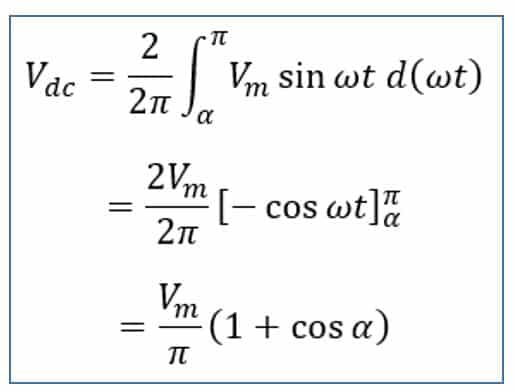
Average or DC Output Voltage
The average or DC output voltage is;
| Supply Voltage vs=400 sin ωt | Maximum value(Vm) =1.414 Vs | Firing angle(α) | Output DC Voltage(Vdc)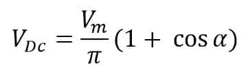 |
| vs=400 sin ωt | 622 | 0 | 396.28 |
| vs=400 sin ωt | 622 | 30 | 369.72 |
| vs=400 sin ωt | 622 | 60 | 297.21 |
| vs=400 sin ωt | 622 | 90 | 198.14 |
| vs=400 sin ωt | 622 | 120 | 99.07 |
| vs=400 sin ωt | 622 | 150 | 26.55 |
| vs=400 sin ωt | 622 | 180 | 0 |
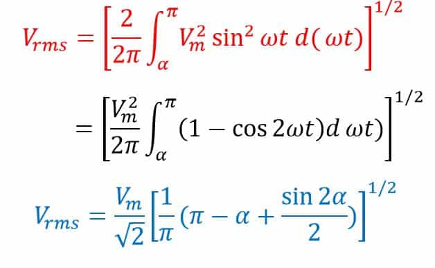
RMS Output Voltage
RMS Output Voltage of Single Phase Semi Converter is;
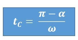
Turn Off Time
The circuit turn off time( in seconds) for a single-phase half controlled converter is;
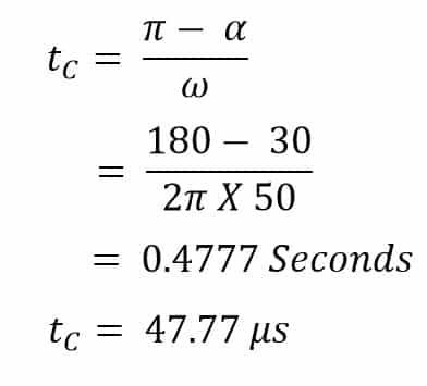
For example, if the firing angle of SCR is 30 degrees, the turn off time of the SCR is;
Read Next: