The varactor diode is a type of diode whose internal capacitance depends on the reverse voltage. The junction capacitance varies with variation in the reverse voltage, and therefore it is also called a varicap diode. The varactor diode stores the charge in the reverse bias.
In many circuits, some applications employ the voltage-variable properties of reverse-biased p-n junctions. A p-n junction designed specifically for such purposes is called a varactor diode.
The varactor diode is an acronym for the carriable reactor, which is also called
- Varicaps
- Tuning diode
- Voltage variable capacitor diode
- Parametric diode
- Variable capacitor diode
The depletion region of the p-n junction acts as the dielectric material between the plates of a capacitor. The variation in the width of the depletion region with the bias gives this type of diode the behavior of a variable reservoir by changing its capacitance.
The varicap diodes have a variable capacitance that varies with the reverse voltage applied. Therefore, it is necessary to understand in advance how variable capacitors work.
Symbol of Varactor Diode
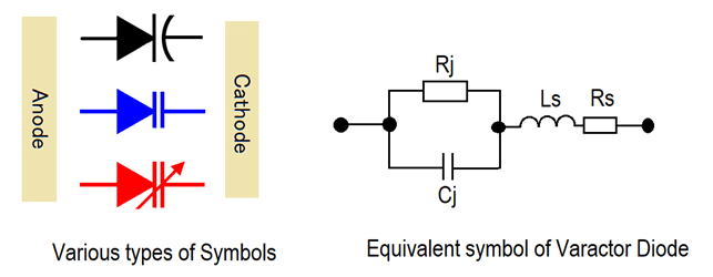
A varactor diode is not a perfect capacitor but an integration of several dependent elements in it. The equivalent circuit consists mainly of a variable capacitance called junction capacitance Cj. A resistance Rj represents the junction resistance, and is parallel to Cj. Apart from these, there is an inductance and resistance in series with parallel combinations of junction elements.
Working Principle of Varactor Diode
A capacitor has two conducting plates separated by a dielectric medium, one of which is connected to a positive voltage and the other to a negative voltage. Since the dielectric medium does not allow charge flow, charge accumulates on the surface of the plates known as capacitance.
The capacitance depends on several factors, including the space between the plates. Its capacitance is inversely proportional to the space between the plates. This principle of operation of variable capacitors is used in varicap diodes.
Operation of Varactor diode
A varactor diode is a PN junction formed by the junction of a P-type semiconductor layer and an N-type semiconductor layer. The P-type layer has mostly positive charges and the N-type layer has mostly negative charges.
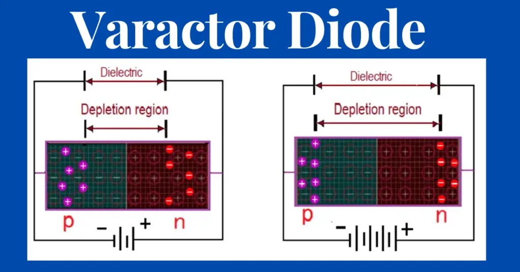
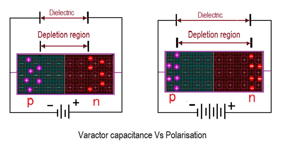
The charges combine in the middle, neutralizing each other and forming a space between the layers called the depletion regions. The depletion region is free but does not allow these carriers t flow unless an electric potential is applied.
The overall structure formed seems a capacitor whose capacitance depends on the width of the depletion region.
The depletion concentration of conventional PN diode and varactor diode is the doping concentration. In a conventional diode doping concentration is uniform, whereas, in a varicap diode, the concentration is low near the junction and decreases towards the outer terminals.
Forward bias Varactor Diode
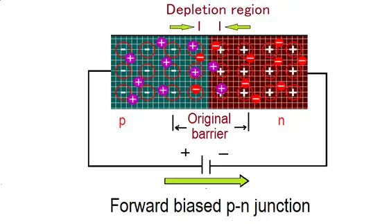
When the varactor diode is forward-biased, the anode is connected to the positive terminal and the cathode to the negative terminal of the voltage source. Upon applying a potential, the width of the depletion region decreases and eventually becomes thinner as shown in the above figure, and a large current flows through the diode. Therefore, the varicap diode is not used in forward bias because it carries current.
Reverse bias Varactor Diode
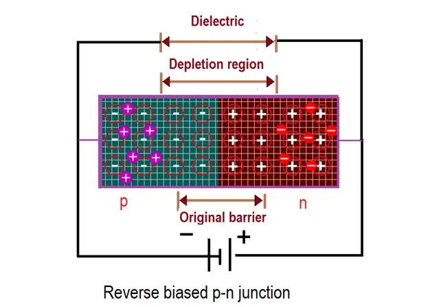
When the varactor diode is connected in reverse bias, the anode is connected negative and the cathode is connected to the positive terminal of the voltage source. An applied reverse voltage moves the charge away from the junction, widening the depletion region. As the reverse voltage is increased, thereby depletion region also gets increased. Therefore, the applied voltage can control the width of the depletion region.
Working of Varactor diode
The structure resembles that of a capacitor where the semiconductor layer is two charge-storing conductive plates, whereas, the depletion region is the dielectric gap between them. The capacitance of the PN junction is called the junction capacitance.
The charge is stored in the opposite layer given by reverse bias. As the depletion width decreases, more charge is stored. That is the capacitance increases. As the depletion width increases, less charge and capacitance of the varactor diode can be varied by varying the reverse voltage.
Therefore, the variable capacitor equation can be used to calculate the capacitance of the varactor diode. The expression for the junction capacitance of a varactor diode is given by

Where,
Cj = Junction capacitance
ε = Dielectric constant of the semiconductor
A = Cross-sectional area of the joint
D = Width of the depletion region.
Varactor diodes are used as capacitors to store, and not conduct charge. It conducts when forward-biased and blocks (stores) the charge when reverse-biased. Therefore, varicap diodes are used only in reverse bias and never in forward bias.
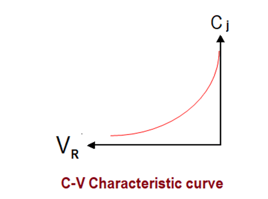
Characteristic Curve – Capacitance-Reverse bias Voltage
Conventional diodes have voltage-current (V-I) is an important characteristic. In the case of varactor diodes, capacitance-voltage (C-V) is the most important electrical characteristic.
From the below figure, it can be seen that the capacitance (Cj) decreases by varying the magnitude of the reverse voltage (VR) as a function of the width of the depletion region, d. While manufacturing them, the doping levels can be controlled to achieve a particular C-V curve.
Advantages of Varicap Diode
- The main advantage is that the capacitance can be easily controlled by varying the applied voltage.
- Varicap diodes generate less noise compared to other P-N junction diodes. Therefore, in varactor diodes, the power loss due to noise is low.
- They are much smaller, and less weight.
- It is more reliable than another P-N diode.
- It is a low-cost diode, so its use in various applications is economical.
Disadvantages of Varicap Diode
- These are specially designed to work in reverse bias mode, it is of less importance when operating in direct bias.
- Its reverse voltage must not exceed the breakdown voltage, otherwise leads to damage.
Applications of Varactor diode
Some applications of the varicap diodes are as follows.
RF system – The varactor diode is widely used in many designs in Radio-Frequency (RF) systems. An applied control voltage can vary the capacitance within a circuit using varicap diodes. This gives them an exceptional capacity because varactor diodes are used in the RF industry.
Radio receivers – Varicap diodes are used in Radio receivers for tuning.
Frequency multiplier – It is used in the phase-locked loop for frequency modulation. Varactor diodes help achieve frequency modulation. The varicap diodes play a vital role in communication devices.
Parametric Amplifiers – The varicap diode is used in parametric amplifiers as an important component. These diodes are used in many circuits and two main sectors.
RF Filters – It is possible to tune filters using varactor diodes. Tracking filters may be required in front-end receiver circuits where the filters are enabled to track the frequency of the received signals.
Voltage-Controlled Oscillators (VCOs) – VCOs are used for many applications and the oscillators within a phase-locked loop are the main region. Voltage-controlled oscillators (VCOs) are present in almost all wireless receivers and radios.