In this article, we will discuss the power MOSFET structure and its characteristics. The MOSFET is an important power electronics device developed by combining MOS technology and areas of field-effect transistor concept.
What is a MOSFET?
- It is a three-terminal device of the drain, gate, and source.
- The circuit symbol of MOSFET is given below
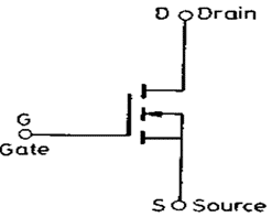
- Arrow indicates the direction of electron flow.
- MOSFET is a voltage-controlled device.
- MOSFET is a unipolar device as a current through MOSFET depends upon the majority- carriers.
- For MOSFET gate terminal is the control terminal, where the gate current is very low. This is because the gate circuit impedance is very large. This large impedance permits the MOSFET gate to be driven directly from the microelectronics circuit.
- Power MOSFETS are generally applicable for low-power high-frequency converters.
- Power MOSFETS are of two types n-channel enhancement type and p-channel enhancement type MOSFET. n-channel MOSFET is used commonly because of the high mobility of electrons.
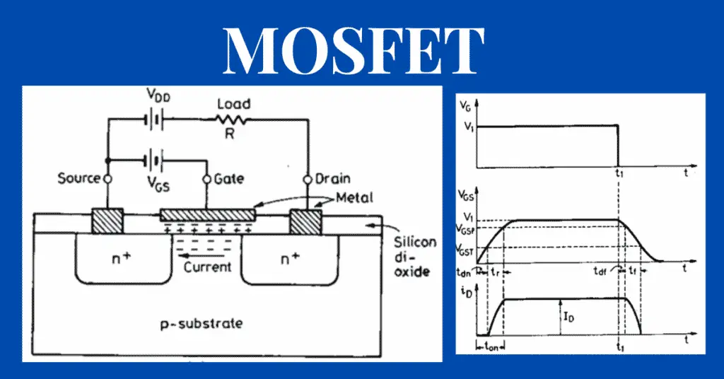
STRUCTURE OF MOSFET
A simplified planar structure of n-channel MOSFET is given below.
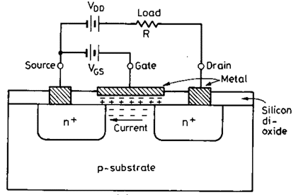
On P-substrate two heavily doped n+ regions are diffused as shown in the above figure. An insulating layer of silicon dioxide (Sio2)is grown on the surface. Now, this insulating layer is etched in order to embed metallic sources and drain terminals. Note that n+ regions make contact with the source and drain terminal as shown. A layer of metal is also deposited on Sio2 so as to form the gate of MOSFET.
GATE circuit decides the state of MOSFET. When the gate circuit is open the current through the MOSFET (drain to source) is zero. Because one n+-p reverse biased. The Load is connected between the drain and source.
When a positive voltage is given to the gate an electric field is established as shown in the figure, eventually, a layer of negative is formed in a p-substrate region in between two n+ layers. In between the layer of positive charge and negative charge Sio2 layer acts as a dielectric. These negative charges form an n-channel and current flows as shown in the figure. If the positive voltage of the gate increase then electron concentration in the n-channel increases which increases the current ID( Drain to source) Drain current is enhanced with increase of gate voltage that is why it is called an enhancement type MOSFET
One disadvantage of the n-channel MOSFET is that on-state resistance is high which leads to one-state power loss. That is the reason MOSFET is preferred for low-power applications.
Characteristics of MOSFET
There are three types of static characteristics of MOSFET.
Transfer characteristics
Transfer characteristics is the plot between drain current and gate to source voltage (ID Vs Vgs).
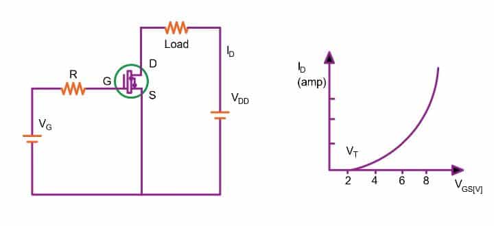
VT is the threshold voltage, which is the minimum voltage required to start the flow of drain current. The threshold voltage is of the order of 2 to 3 volts.
Output (O/P) Characteristics
Power MOSFET output characteristics are shown in the figure below.
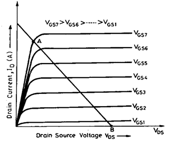
From characteristics, it can be concluded that at the low value of VDS the current is linear i.e the on-state resistance is constant. But at a high value of VDS, the current remains constant and varies with VGS. The load line intersects between A and B.
Switching Characteristics
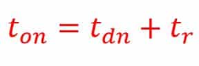
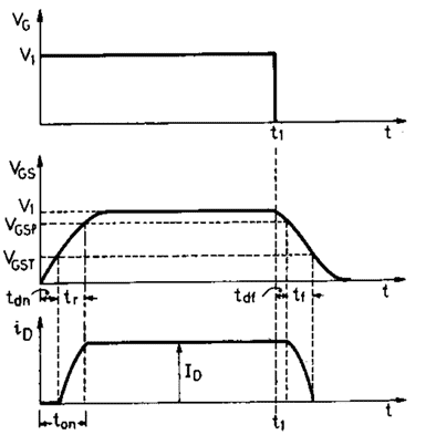
The switching characteristics of a power MOSFET are influenced to a large extent by the internal capacitance of the device and the internal impedance of the gate drive circuit. At turn-on, there is an initial delay tdn during which input capacitance charges to gate threshold voltage VT. Here tdn is called turn-on delay time. There is a further delay time called rise time (tr), during which gate voltage rises to VGSP, a voltage sufficient to drive the MOSFET into the on-state. During rise-time, the current rises from zero to the drain current (ID). Thus, the total turn-on time can be written as;
The turn-on time can be reduced by using the low impedance gate drive source.
As MOSFET is a majority carrier device, the turn-off process is initiated soon after the removal of gate terminal voltage at time t1. The turn-off delay time tdf, is the time during which input capacitance discharges from overdrive gate voltage V1 to VGSP. The fall time, tf is the time during input capacitance discharges from VGSP to the threshold voltage. During fall time drain current falls to zero. So when VGS is less than threshold voltage then MOSFET goes off. The switching characteristics are given below.
Power MOSFET are widely used in SMPS and their ratings are 500V and 140 A.
Comparison between MOSFET & BJT
- Power MOSFET has a higher on-state voltage drop i.e high on-state resistance compared to BJT. So, on-state power loss is more in MOSFET compared to BJT. Switching loss is lesser in MOSFET compared to BJT. So MOSFET is applied in high-frequency power circuits.
- BJT is current controlled device and MOSFET is voltage controlled device.
- MOSFET has a positive temperature coefficient for resistance. This makes the parallel operation of MOSFET easy. BJT has a negative temperature coefficient which decreases on state resistance due to which current sharing resistor is required for parallel operation of BJT.
- In MOSFET secondary breakdown does not occur, because it has a positive temperature coefficient which decreases current with time but in the case of BJT, the negative temperature coefficient of the resistor results in rise in on-state current which creates hotspots and eventually breakdown of BJT.
- Power MOSFET has higher on-state losses with a high voltage rating.
- Ratings of BJT used are 1200V and 800A whereas MOSFET used are of 500V and 140A.
Combining both the BJT and MOSFET a new device is developed called IGBT.