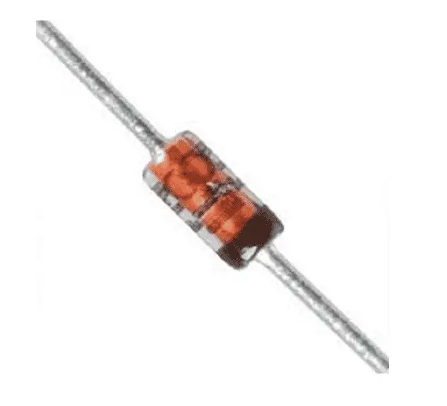
The change of forward and reverse biasing of the diode makes the diode a switch. The diode is a two-terminal semiconductor device that has a PN junction. When the PN junction is forward-biased, it acts as a close switch, and it acts as an open switch when the junction is in a reverse-biased state. Thus, when the state of the PN junction changes from reversed biases to forward bias or vice versa, the diode acts as a switch. The PN junction diode acts as an electrical switch.
Working of Diode as a Switch
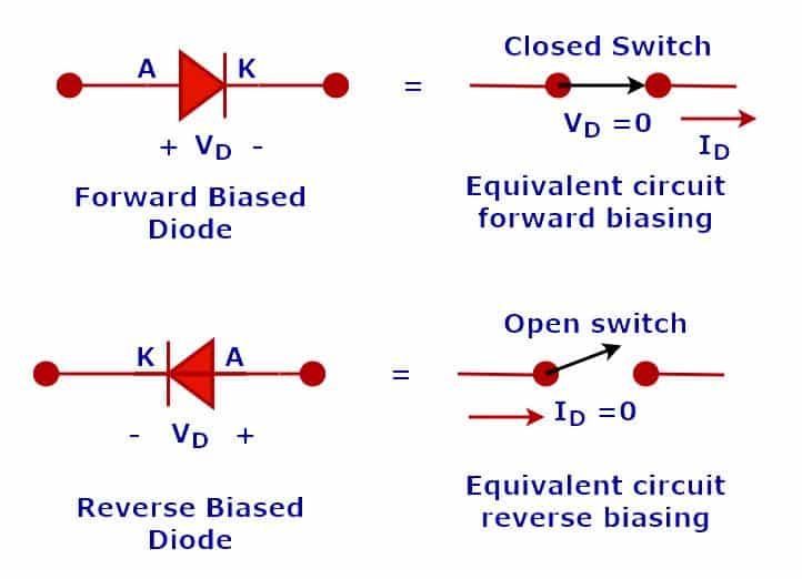
The principle of working of a diode as a switch is nothing but the forward and reverse biasing of the diode. When a forward voltage exceeds the cut-in voltage of the PN junction diode, the current flows through the junction. Thus, the diode junction becomes a short circuit. The diode comes in the reverse bias when the voltage at the diode’s anode is more negative than the voltage at the cathode. In this condition, the diode junction is an open circuit.
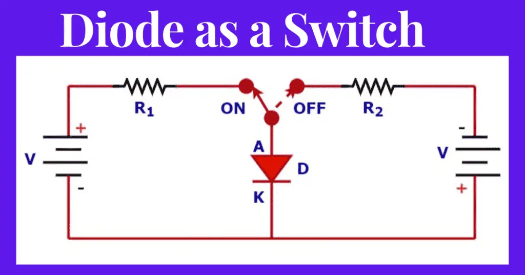
Let us understand how the diode works as a switch with the help of the diagram below.
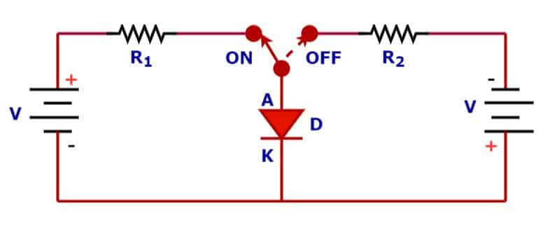
A diode has a PN junction. In a diode, the P-region has lightly doped holes as the majority carriers, and the N- region has highly doped electrons as the majority carriers. When the switch is at the ON position, the anode of diode D gets a positive supply, and the cathode of diode D gets a negative supply. In this condition, the diode gets forward biasing, and it starts conducting.
Now, when the switch position changes from ON to OFF state, the anode of the diode gets the negative voltage at the anode. Under this condition, the current flowing in the forward bias state drops to zero, and the diode becomes an open circuit. Here, note that the diode forward current does not fall to zero instantly, but it takes some time. This time is called the reverse recovery time. Now, the diode draws negligible leakage current in the reverse bias.
A ringing phenomenon occurs when the diode transitions from a forward-biased to a reverse-biased state. When a reverse voltage is applied to the diode after forward current flow, reverse current flows for an instantaneous moment rather than instantly switching off. This reverse current is called recovery current.
During the flow of the recovery current, the recovery current may create a few oscillations. These oscillations are called ringing. The ringing condition causes power loss and it is desirable to have minimum ringing.
Diode Switching Times
Switching times are a crucial aspect of an ideal switch. It should have the shortest possible turn-on and turn-off times. Now, let us understand the switching times of a diode in detail.
While changing the bias conditions, the diode experiences a transient response when transitioning from forward bias to reverse bias and vice versa. The duration of response under transient conditions is a crucial factor for an electrical switch.
To understand the diode switching times let us analyze what happens when voltage is applied to a switching PN diode.
Mechanism behind Diode Switching Times
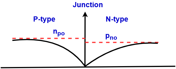
The concentration of minority charge carriers decreases exponentially as the distance from the junction increases. When voltage is applied in a forward-biased condition, the majority carriers from one side move to the other side. Once they cross over, they become minority carriers on the opposite side. The concentration of these carriers is highest at the junction.
For example, in an N-type material, forward bias causes excess holes to enter. These holes add to the existing minority carriers in the N-type material.
Now, let’s define some notations:
- Majority carriers in P-type (holes) = Ppo
- Majority carriers in N-type (electrons) = Nno
- Minority carriers in P-type (electrons) = Npo
- Minority carriers in N-type (holes) = Pno
During forward bias condition: The minority carriers are more concentrated near the junction and decrease as the distance from the junction increases. The graph below illustrates this behavior.

Excess minority carrier charge in P-type = Pn−Pno, where Pno is the steady-state value.Excess minority carrier charge in N-type = Np−Npo, where Npo is the steady-state value.
During reverse bias condition: The majority carriers do not conduct current through the junction. As a result, they do not contribute to current flow. For a brief moment, the switching diode behaves like a short circuit in the reverse direction.
However, the minority carriers cross the junction and conduct current. This current is known as Reverse Saturation Current. The following graph illustrates this condition during reverse bias.
In the figure above, the dotted line shows the equilibrium values.
The solid lines represent the actual values. The current from the minority charge carriers is strong enough to conduct. As a result, the circuit remains ON until this excess charge is removed.
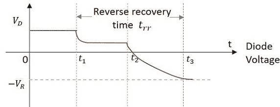
The time needed for a diode to switch from forward bias to reverse bias is called Reverse Recovery Time (trr). The following graphs provide a detailed explanation of diode switching times.
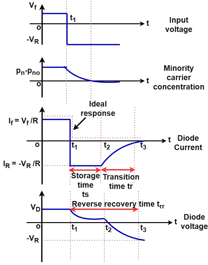
From the figure above, let’s analyze the diode current graph. At t1, the diode switches suddenly from the ON state to the OFF state. This period is called Storage Time. Storage time is the duration needed to remove the excess minority carrier charge. During this time, a significant negative current flows from the N-type material to the P-type material. This negative current is:
The next time period is called Transition Time, which occurs between t2 and t3. Transition time is the duration required for the diode to fully reach the open-circuit condition. After t3, the diode enters a steady-state reverse bias condition.
Before t1, the diode was in a steady-state forward bias condition.
The total time taken for the diode to become fully open-circuited is:
Reverse Recovery Time(trr)=Storage Time(Ts)+Transition Time(Tt)
On the other hand, switching from OFF to ON takes less time. This shorter time is called Forward Recovery Time. Reverse recovery time is longer than forward recovery time. A diode functions as a better switch when its reverse recovery time is minimized.
Definitions
Let’s briefly review the definitions of the diode switching time periods discussed.
Recovery Time
The recovery time of a diode is the total time it takes for a diode to switch from one state (either forward-conducting or reverse-blocking) to the opposite state. Thus, the time taken before the diode recovers its steady state is called Recovery Time.
Forward Recovery Time(tfr)
Forward Recovery Time is the time required for a diode to transition from a reverse-biased (non-conducting) state to a forward-biased (conducting) state.
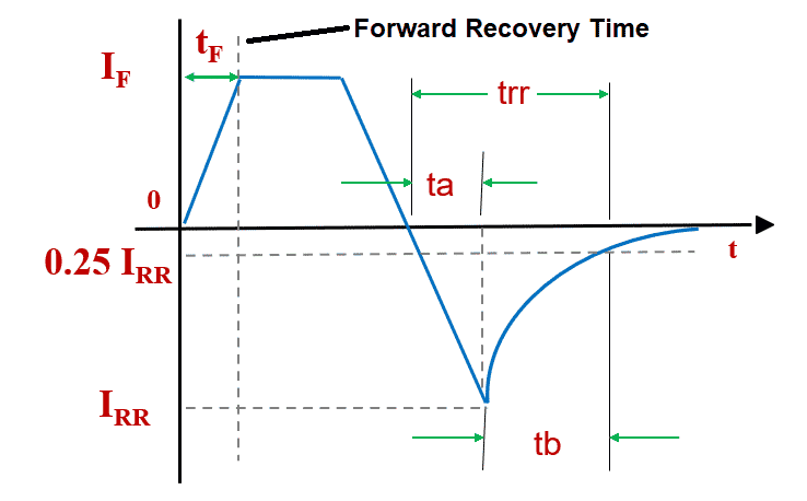
On application of forward biasing in an OFF state diode, the voltage across the diode instantly shoots up to about 1–2 volts before settling down to its final value of 0.7 volts because the diode needs some time to start conducting because of the charge carrier buildup in the depletion region. The time taken to cross 10% of the final value to peak and fall to the final value is the forward recovery time. It is an important consideration in the selection of diodes for SMPS. For fast-switching diodes, it is about 50 ns.
Reverse Recovery Time (trr)
The reverse recovery time is the duration taken by a diode to switch from a forward-biased (conducting) state to a reverse-biased (non-conducting) state.
When the forward current is abruptly interrupted and a reverse voltage is applied, the diode does not instantly cease conducting due to the residual charge carriers within the junction. The reverse recovery time is the duration necessary to remove these excess carriers. The current flows through the diode after the application of the reverse bias is called reverse recovery current.
The recovery time is in order from a few nanoseconds to a few microseconds or even more. It all depends on the device and the current levels. The main reason for this reverse recovery current and reverse recovery time is that minority charges require time to recombine with the majority charges in the depletion region. This causes a significant power loss in switching regulators.
Storage time(ts)
The period for which the diode remains in the conduction state, even in the reverse-biased state, is called Storage time.
Transition Time (tt)
The time required for the current to reverse and stabilize at its reverse value.
Summary of Diode Switching Times
- Storage time − The storage time of a diode is the time it takes for a diode to stop conducting current after the forward bias voltage is removed and before it starts blocking current in the reverse-biased state.
- Transition time − The transition time of a diode is the time it takes for the diode to change from conducting in the forward direction to fully blocking in the reverse direction after the forward current has dropped to zero.
- Reverse recovery time −The Reverse recovery time of a diode is the time it takes for the diode to switch from conducting in the forward direction to fully blocking in the reverse direction after the forward current has been removed and a reverse voltage is applied.
- Forward recovery time − The forward recovery time of a diode is the time it takes for the diode to start conducting fully when a forward voltage is applied after it has been in a non-conducting state.
Factors Affecting Switching Times
The following factors affect the diode switching times, such as
- Doping Levels: Increased doping levels reduce the reverse recovery time by decreasing the number of stored charge carriers.
- Diode Type: Schottky diodes, for instance, exhibit significantly shorter recovery times compared to conventional PN junction diodes due to their metal-semiconductor junction.
- Junction Capacitance: Higher junction capacitance can lead to longer recovery times and increased diode switching times.
- Temperature: Higher temperatures can prolong the reverse recovery time as they increase the lifetime of the charge carriers.
Applications of Diode Switching Circuits
The diode is used as a switch for the following applications.
- High-speed rectifying circuits
- High-speed switching circuits
- RF receivers
- General-purpose applications
- Consumer applications
- Automotive applications
- Telecom applications, etc.
Read Next: