A tunnel diode is a high-performance electronic component. It is used in high-speed electronic circuits. A tunnel diode is a semiconductor device composed of two oppositely charged p-n regions separated by a very narrow neutral region. The electrical current can be controlled over a wide range by varying the bias voltage, which changes the energy of the tunneling electrons.
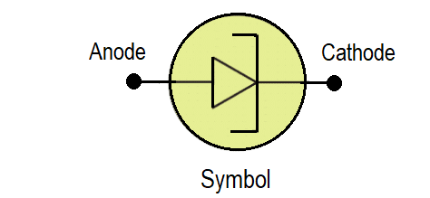
The symbol of the tunnel diode is given below.
An important characteristic of the tunnel diode is its negative resistance over a given forward-bias voltage range. When resistance is negative, current decreases with increasing voltage. Consequently, the tunnel diode can function as an amplifier, oscillator, or bistable.
This article provides an overview of tunneling and how it works.
History of Tunnel Diode
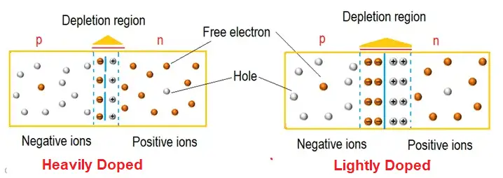
Leo Esaki, a Japanese physicist discovered tunnel diode in the year 1958. His research on heavily doped semiconductor materials (like Ge-Si) resulted in the discovery of a Tunnel diode. During his research, he found that when a semiconductor diode is heavily doped with impurities, it generates negative resistance.
Leo Esaki won the prestigious Nobel Prize in Physics in the year 1973 for pioneering work on his invention and design. Tunnel diodes are one of the important solid-state electronic components.
The tunnel diode is also called Esaki diode in honor of its Japanese inventor Leo Esaki for his work on tunneling phenomena.
Construction of a Tunnel Diode
Germanium (Ge), gallium antimonide (GaSb), and Gallium arsenide (GaAs) are used to manufacture the tunnel diode the semiconductor material silicon (Si) is not suitable and preferred in the manufacture of Tunnel diodes.
The tunnel diode is constructed from two semiconductors: a p-type (anode) and an n-type (cathode). Generally, an anode is similar to an electrode and has a positive charge that attracts electrons, while a cathode is a negatively charged electrode that generates electrons.
A heavily doped semiconductor diode will have a thinner depletion zone than a lightly doped one, shown in the figure below. It means that the diode’s current flow will decrease once the voltage increases.
V-I Characteristics of a Tunnel Diode
Using the below graph, one can understand the operation of the tunnel diode when it is forward-biased. When applying an initial voltage, its current progressively increases until reaching a maximum or peak current (Ip), at this point it has a peak voltage (Vp). Once the high voltage is applied to this diode, the current value will decrease.
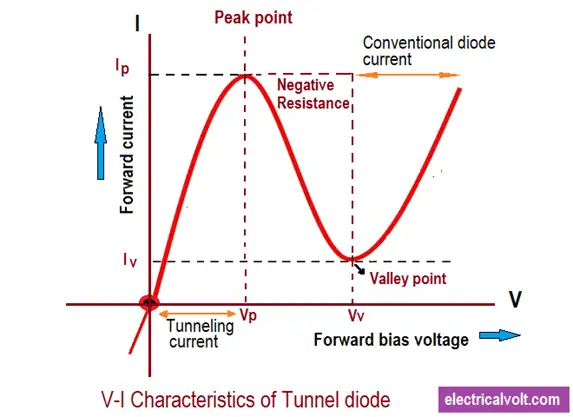
Increasing the voltage Vp will produce a decrease in current until reaching a minimum current, this region is called negative resistance. This smallest current that decreases is called the valley point (Iv) and the voltage at that point is called the valley voltage (Vv). The tunnel diode has the characteristic of changing its current curve when its voltage increases. This negative resistance curve is called the tunneling effect.
If the voltage continues to increase going to a higher value of Vv, then the current will start to increase progressively proportional. In this region, the diode acts as an ordinary conventional diode.
Working of Tunnel diode – Negative resistance zone
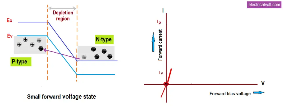
The origin of the zone of negative resistance can be better understood by analyzing the diagram of energy bands of the tunnel diode.
The below figures show the band diagram for the tunnel diode where four aspects can be highlighted during the polarization of the device. The shaded areas represent the energy states by electrons in the band. Valence band and conduction band for p-type and n-type semiconductors respectively.
Step 1:
When there is no polarization on the diode, the energy levels in the band of conduction and valance band are at the same height,
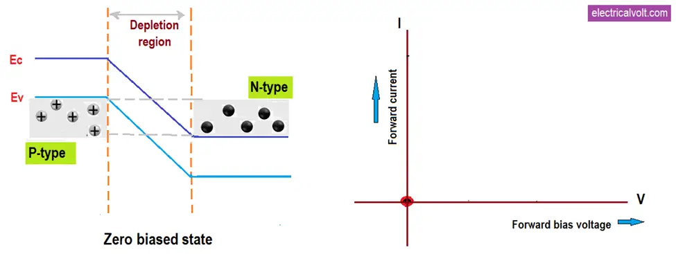
Once the electrons are given energy from an external source they promote the modification in said levels, however, the energy possessed by the electrons in the n-region is not enough to overcome the energy barrier and go to the semiconductor type -p.
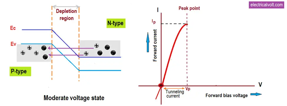
Step 2 :
When a small voltage is applied across the junction the energy levels in the p-type material decrease compared to that of the n-type material.
So, electrons in the conduction band of the n-type semiconductor observe available spots in the p-type material. Therefore, the movement of electrons in the semiconductor is promoted. The n-type occupies the empty places in the semiconductor p-type, all this is done by means of the tunneling of electrons.
Step 3:
However, when the peak current (Ip) is reached, the number of available places is disturbed, causing the current to decrease and thus giving rise to the zone of negative resistance. This will continue until the available states in the band are completely filled. The valence of the p-type semiconductor and with it the current will decay to volt-ampere characteristics illustrated previously.
Step 4:
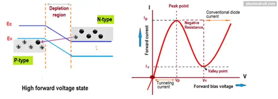
Once the zone of negative resistance is exceeded, it means that the electrons already have enough energy to overcome the energy barrier, and therefore the current increases exponentially with the applied voltage with which volt-ampere characteristics are observed similar to those of conventional diodes.
Advantages of Tunnel diode
- Tunnel diodes are suitable for microwave RF applications because of their high speed.
- Manufacturing is simple.
- Used as a switching device as the response is quick.
- Its performance remains stable over long periods and works for a long time, whereas other semiconductor devices may degrade.
- The tunnel diode is inexpensive, and the noise is less.
- Strong doping results in resistance to radiation.
- Lower power consumption.
- Due to the large number of charge carriers, it is a diode, and the current flow responds very quickly to voltage changes.
- There is a significant overlap between two bands, valence, and conduction resulting in a large current supply at a small reverse voltage value. This is a very useful property as a frequency converter. It generates a negative resistance characteristic that is used in reflection oscillators and amplifiers.
- It generates a negative resistance characteristic that is used in reflection oscillators and amplifiers.
Disadvantages
- Reverse-biased tunnel diodes are unsuitable rectifiers due to their high leakage current.
- It can only be used in special circuits where their tunneling effect is helpful. These diodes are held a bias voltage somewhere between peak, and trough voltage levels to exploit tunneling.
- It is always in forward-biased polarity (positive anode and negative cathode).
- A tunnel diode is a low-voltage output (below 1 V) level, that cannot be used in large integrated circuits. Hence, its application is limited.
Applications
- The most common application is simple high-frequency oscillator circuits, up to the gigahertz (GHz) range.
- Used to build amplifiers and oscillators.
- They are used in microwave circuits.
- Used in satellite communication equipment.