A Schottky diode is a metal-semiconductor junction (M-S) diode that has less forward voltage drop than the P-N junction diode and can be used in high-speed switching applications. The forward voltage drop of the silicon P-N junction diode is 0.7 volt.
The forward voltage drop of the Schottky diode is 0.3 volts, similar to that of the germanium P-N junction diode. However, germanium diodes are rarely used because their switching speed is very low compared to that of Schottky diodes.
In the P-N junction diode, the conduction takes place through the majority carriers. However, if the minority carrier is injected into the region, it is difficult to remove these charge carriers, and because of these stored charges, the device takes more time to go into the off state.
The turn-off time of the device increases when the charges get stored in the depletion region. The turn-off time of the Schottky diode is very low as compared to the P-N junction diode, and this feature of the Schottky makes it suitable for high-frequency applications.
The Schottky diode is connected across the collector and the base junction to prevent the BJT from going into saturation and to improve the switching characteristic of the BJT. The logic family using this technology is called Schottky TTL.
Schottky Diode Symbol
The symbol of the Schottky barrier diode is given below.

Schottky Diode Working Principle
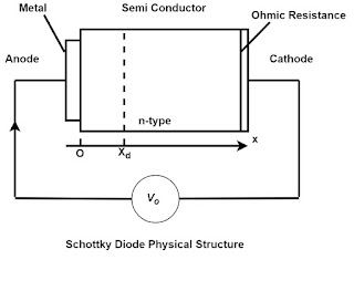
The Schottky diode has a metal-semiconductor junction. Metals such as aluminum or platinum replace the P-type semiconductor. The N-type semiconductor acts as a cathode, and the metal side acts as the anode.
The Schottky diode is named after German physicist Walter H. Schottky. A Schottky diode is also known as a Schottky barrier diode, a surface barrier diode, a majority carrier device, a hot-electron diode, or a hot carrier diode. Schottky diodes are widely used in radio frequency (RF) applications.
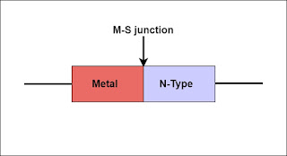
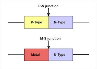
When a metal like aluminum or platinum is joined with an N-type semiconductor, a junction is formed between the metal and N-type semiconductor. This junction is known as a metal-semiconductor junction or M-S junction.
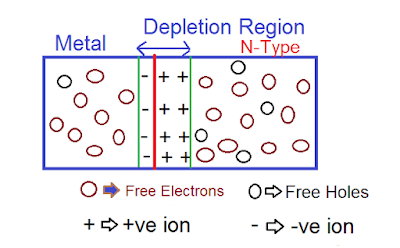
A metal-semiconductor junction formed a depletion layer known as a Schottky barrier. The Schottky diode can switch on and off much faster than the P-N junction diode because the junction capacitance of the Schottky diode is very low compared to the junction capacitance of the P-N junction diode.
Also, the Schottky diode produces less unwanted noise than the P-Njunction diode. These two characteristics of the Schottky diode make it very useful in high-speed switching power circuits.
The voltage drop across a silicon P-N junction diode is 0.6 to 0.7 volts. On the other hand, a Schottky diode has a lower voltage drop of 0.2 to 0.3 volts, which leads to higher efficiency.
Operation of Schottky Diode
The free electrons from the n-type semiconductor move from the n-type semiconductor to metal during the combination process when the Schottky diode is unbiased.
V-I Characteristics Of Schottky Diode
The V-I characteristics of a Schottky barrier diode are as given below.
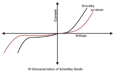
- The forward voltage drop of the Schottky barrier diode is very low compared to a normal PN junction diode.
- The forward voltage drop ranges from 0.3 volts to 0.5 volts.
- The forward voltage drop increases with the increase of T N-type semiconductor concentration.
- The V-I characteristics of a Schottky barrier diode are steeper than that of a normal PN junction diode due to the high concentration of current carriers.
Applications Of Schottky Diode
Schottky diodes are used for the following purposes.
- Voltage clamping applications and prevention of transistor saturation
- Used for RF applications.
Advantages Of Schottky Diode
- Low turn-on voltage: The turn-on voltage for the diode is between 0.2 and 0.3 volts. For a silicon diode, it is against 0.6 to 0.7 volts from a standard silicon diode.
- Fast recovery time: A fast recovery time means a small amount of stored charge that can be used for high-speed switching applications.
- Low junction capacitance: It occupies a very small area after the result obtained from the wire-point contact of the silicon since the capacitance levels are very small.