Silicon is a semiconductor material with a unique characteristic – it has a number of free electrons that is less than a conductor but more than an insulator. Because of this, silicon is widely used in the field of electronics. Silicon has two energy bands: the conduction band and the valence band. The valence band is formed by a series of energy levels with valence electrons in the solid. At an absolute temperature of 0 Kelvin, the energy levels of the valence band are filled with electrons. When the electrons are in the valence band and have the maximum energy, no current flows due to these electrons.
The conduction band is the higher energy level band and represents the minimum amount of energy. This band is partially filled with electrons known as free electrons, as they are able to move anywhere within the solid. These electrons are responsible for the flow of current. There exists an energy gap between the conduction band and the valence band, and this difference in energy is referred to as the forbidden energy gap which determines the nature of a solid.
The properties of a solid, whether it is a metal, insulator, or semiconductor, are determined by the size of its forbidden energy gap. Metals have no gap, insulators have a large gap, and semiconductors have a moderate gap. At a temperature of 300oK, silicon has a forbidden gap of 1.12 eV. In a silicon crystal, covalent bonds exist, and the material is electrically neutral. When an electron breaks away from a covalent bond, it leaves behind a hole. As the temperature increases, more electrons move to the conduction band, creating more holes in the valence band.
Energy Band Diagram of Silicon
The energy band diagram of silicon illustrates the energy levels of electrons in the material. In intrinsic silicon, the Fermi level lies in the middle of the energy gap. When the intrinsic silicon is doped with donor atoms, it becomes n-type and then Fermi level moves higher i.e. closer to the conduction band. When doped with acceptor atoms, intrinsic silicon becomes p-type, and the Fermi level moves toward the valence band.
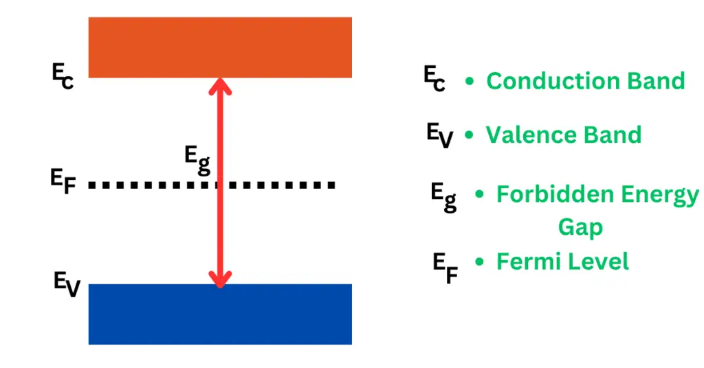
Energy Bands Diagram of Intrinsic Silicon
In intrinsic silicon, the Fermi level lies approximately midway between the conduction band and the valence band. This is because the number of electrons in the conduction band is equal to the number of holes in the valence band, maintaining electrical neutrality. The position of the Fermi level indicates the relative distribution of electrons and holes in the semiconductor. For intrinsic silicon, it being near the center of the Band Gap shows that there are equal concentrations of electrons and holes.
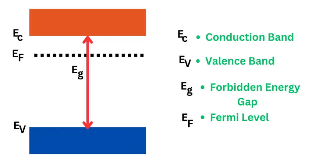
Energy Bands Diagram of Extrinsic Silicon
For n-Type
In n-type silicon, the Fermi level is closer to the conduction band due to the increased number of free electrons. It is positioned above the midpoint of the Band Gap, indicating a higher probability of electron occupancy in the conduction band. The higher Fermi level reflects the increased electron concentration in the conduction band, which enhances the material’s electrical conductivity. This shift is a direct result of the donor doping process.
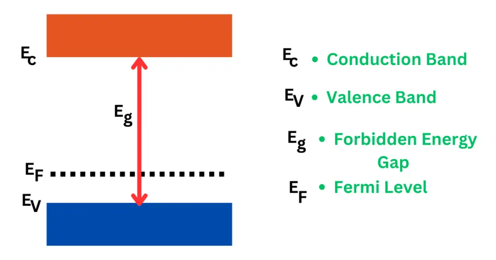
For p-Type
In p-type silicon, the Fermi level is closer to the valence band due to the increased number of holes. It is positioned below the midpoint of the Band Gap, indicating a higher probability of hole occupancy in the valence band. The lower Fermi level reflects the increased hole concentration in the valence band, enhancing the material’s electrical conductivity. This shift is a direct result of the acceptor doping process.
pp