The NOT gate, also known as an inverter gate, is one of the basic logic gates used in digital electronics. It performs the inversion operation by producing the opposite logic state at its output. Because of its simple operation and wide range of applications, the NOT gate is an essential building block in digital circuits, microprocessors, memory devices, and control systems.
In this article, you will learn what a NOT gate is, its logic symbol, truth table, Boolean expression, electrical equivalent circuit, transistor implementation, universal gate implemenation, commonly used ICs, and practical applications.
What is a NOT Gate?
In digital electronics, the NOT gate has a single input and a single output. It gives a high output (Logic 1) when its input is low (Logic 0), and it gives a low output (Logic 0) when its input is high (Logic 1). Therefore, it operates as an inverter, i.e. converts high into low or low into high.
Symbol of NOT Gate
The logic symbol of the NOT gate is shown in the figure below. It has one input, represented by A, and one output, represented by Y. The output Y is always the complement (inverse) of the input A. The small circle, or bubble, at the output of the symbol is called the inversion bubble. It indicates that the output is the inverted form of the input signal.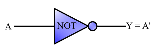
Operation of NOT Gate
The NOT gate performs the logical inversion operation by producing the complement of the input signal. Its operation is as follows:
- If the input is 0 , the output becomes 1
- If the input is 1 , the output becomes 0
Boolean Expression
A Boolean expression represents the logical relationship between the input and output of a logic gate. The Boolean expression of the NOT gate is given below.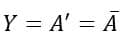
Here, A is the input variable and Y is the output variable. The complement is represented by a bar (Ā) or an apostrophe (A’).
Truth Table of NOT Gate
The truth table shows the output produced by the NOT gate for every possible input condition. Since a NOT gate performs the inversion operation, the output is always the complement of the input. Thus, an input of 0 produces an output of 1, while an input of 1 produces an output of 0. The truth table for the NOT gate is as follows:Input (A) Output (Y = A’) 01 1 0
Use of Active-Low Input Bubble
In digital logic, the active-low input bubble is shown as a small circle at the input of a gate symbol, indicating that the signal is inverted. In the case of a NOT gate, which already performs inversion, this bubble represents the inversion of the input logic level. Thus, when an input is marked with an active-low bubble, it signifies that the output will always be the complement of the applied input signal.
Implementation of NOT Gate Using Universal Gates
A NOT gate can also be implemented using the two universal logic gates, namely NAND and NOR. The implementation of a NOT gate using these gates is explained below.
NOT Gate Using NAND Gate
A NOT gate can be realized using a NAND gate by connecting all of its input terminals together and applying the input signal to the common connection, as shown in the figure below.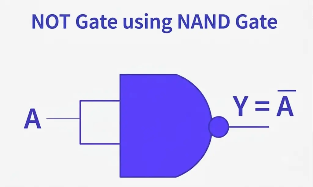
The output of this circuit can be expressed by the following Boolean equation:
Y = A
NOT Gate Using NOR Gate
A NOT gate can also be implemented using a NOR gate. This is achieved by connecting all the input terminals of the NOR gate together and applying the input signal to the common input, as shown in the figure below.
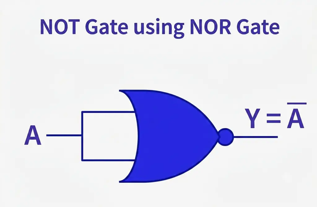
The Boolean expression for this circuit is:
Y = A + A = A
Electrical Equivalent Circuit
The electrical equivalent circuit of the NOT gate is shown in the following figure.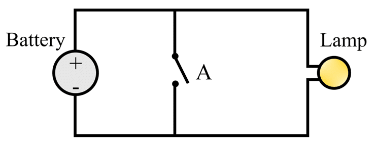
The circuit consists of a battery, a switch, and a lamp. It performs the NOT operation as follows:
- When the switch is open (A = 0): Current flows from the battery through the lamp and returns to the battery, causing the lamp to glow. Therefore, the output is high (Y = 1).
- When the switch is closed (A = 1): The switch provides a low-resistance path, allowing the current to bypass the lamp. As a result, no current flows through the lamp, and it remains OFF. Therefore, the output is low (Y = 0).
Thus, the above circuit performs the inverter (NOT) operation.
NOT Gate Implementaion Using Transistor
The NOT gate can be implemented by using a bipolar junction transistor (BJT). The circuit diagram of a NOT gate using a bipolar transistor is shown in the following figure.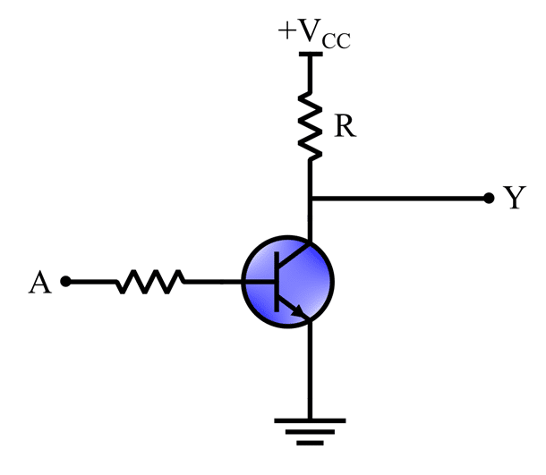
This circuit is also known as a transistor inverter.
When a high voltage (say +5 V) is applied at the input A, the transistor turns ON, and the current flows from +VCC to ground through the transistor, making the output low (Logic 0).
When the input voltage at A is low (0 V), the transistor turns OFF, and the current does not find any path to the ground. Hence, the entire supply voltage (+VCC) will be available at the output Y, making it high (Logic 1).
NOT Gate ICs
The following table provides a list of commonly used inverter ICs in TTL and CMOS logic families:IC Name Logic Family Description 74LS04 TTL Logic Hex Inverting NOT Gate 74LS14 TTL Logic Hex Schmitt Inverting Gate 74LS1004 TTL Logic Hex Inverting Drivers CD4009 CMOS Logic Hex Inverter NOT Gate CD4069 CMOS Logic Hex Inverting NOT Gate
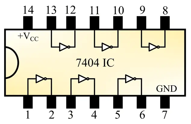
7404 NOT Gate IC
The IC 7404 is a commonly used NOT gate IC available in the market. It contains six NOT gates in TTL logic. The schematic diagram of the 7404 IC is shown in the following figure.
Applications of NOT Gate
- Signal Inversion: The NOT gate is widely used to invert digital signals. When the input is logic high (1), the output becomes logic low (0), and when the input is logic low (0), the output becomes logic high (1). This simple inversion is fundamental in digital circuit design.
- Flip-Flops and Latches: NOT gates are essential components in sequential circuits such as flip-flops and latches. They help in storing binary data by providing feedback and maintaining stable memory states in digital systems.
- Logical Operations and Circuit Design: NOT gates are used in combination with other logic gates to implement complex Boolean expressions and digital logic functions in processors and control systems.
- Automatic Lighting Systems: In automatic lighting systems, a NOT gate helps in switching operations. For example, lights turn ON when it is dark (logic 0) and turn OFF when it is bright (logic 1), making it useful in smart control systems.
- Temperature Detection and Control Systems: NOT gates are used in temperature-based control circuits where sensor outputs are inverted to trigger cooling or heating mechanisms based on environmental conditions.
- Microprocessors and Microcontrollers: The NOT gate is a basic building block in CPUs and embedded systems, where it is used in arithmetic, control, and decision-making circuits.
- Waveform Generation and Signal Processing: In digital electronics and CMOS inverter circuits, NOT gates are used to generate square waves and invert signals for timing and processing applications.
- Digital Communication Systems: NOT gates are used in encoding and decoding circuits where signal inversion is required for data transmission and error handling.
Advantages of NOT Gate
- Simple Design: The NOT gate has a very simple structure with a single input and output, making it easy to implement in digital circuits.
- Fundamental Building Block: It is one of the basic elements used in designing all complex digital systems and ICs.
- Low Cost: NOT gates are inexpensive to manufacture and are widely available in IC form.
- Fast Operation: Due to simple switching, NOT gates operate at high speed in digital circuits.
Disadvantages of NOT Gate
- Limited Functionality: The NOT gate performs only inversion and cannot perform complex logic operations alone.
- Increased Circuit Complexity: More complex functions require multiple gates, increasing circuit size and design complexity.
- Power Consumption in Large Systems: When used in large-scale circuits, multiple NOT gates can contribute to higher power usage.
- Propagation Delay: Like all logic gates, it introduces a small delay during switching, which may affect high-speed digital systems.
Conclusion
The NOT gate, also known as an inverter, is one of the most fundamental building blocks in digital electronics. It performs the simple yet important operation of logical inversion, where the output is always the opposite of the input.
Due to its simplicity, it is widely used in combinational and sequential circuits, including microprocessors, memory elements, control systems, and digital communication systems. Understanding the NOT gate provides a strong foundation for learning more complex logic gates and digital circuit design.
Read Next:
- Logic Gates: Types, Working, Symbols, Truth Tables, Boolean Expressions
- Logic OR Gate-Symbol, Truth Table, and Circuit Diagram
- Logic NOR Gate- Symbol, Truth Table and Circuit Diagram
- Logic AND Gate: Symbol, Truth Table, Working, Circuit Diagram
- Logic NAND Gate- Symbol, Truth Table, Circuit Diagram, Working
- Universal Logic Gate
- Exclusive-OR Gate with EX-OR Gate Truth Table
- XNOR Gate: Symbol and Truth Table
- What is Transistor Transistor Logic (TTL Logic) & Its Working
- IC 741 Op Amp Basics, Characteristics, Pin Configuration, Applications