Schottky Diode is an essential component in modern electronics, known for its efficiency and speed. herefore, it is used widely in switching power supplies, radio frequency systems, and digital circuits.
Its low forward voltage drop and rapid response make it particularly suitable for high-frequency and low-voltage applications.
The Schottky diode is named after German physicist Walter H. Schottky. It is also referred to as a Schottky barrier diode, surface barrier diode, majority carrier device, hot-electron diode, or hot carrier diode.
What is Schottkey Diode?
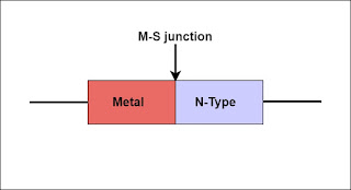
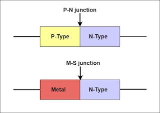
A Schottky diode is a metal-semiconductor junction (M-S) diode that has less forward voltage drop than the P-N junction diode and can be used in high-speed switching applications. The forward voltage drop of the silicon P-N junction diode is 0.7 volt.
Unlike traditional diodes that use a P-N junction, this diode forms a junction between a metal (like aluminum or platinum) and an N-type semiconductor. As a result, this structure results in faster switching speed and lower power loss, making Schottky diodes ideal for power electronics, RF systems, and clamping circuits.
Schottky Diode Symbol
The symbol of the Schottky diode is similar to that of a standard P-N junction diode, but with a slight modification. In the Schottky diode symbol, the vertical bar of the conventional diode is replaced with an “S”-shaped curve, indicating the metal-semiconductor junction. Thus, this unique symbol differentiates it from other types of diodes and helps in easy circuit identification.
The symbol of the Schottky barrier diode is given below.

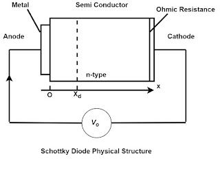
Construction of Schottky Diode
The Schottky diode has a metal-semiconductor junction. Metals such as aluminum or platinum replace the P-type semiconductor. The N-type semiconductor acts as a cathode, and the metal side acts as the anode.
This unique metal–semiconductor configuration eliminates minority carrier injection, resulting in lower junction capacitance and faster switching performance compared to conventional P-N junction diodes.
Schottky Diode Working
The working of a Schottky diode depends on the movement of electrons between the metal and the n-type semiconductor. Its behavior changes based on whether it is unbiased, forward biased, or reverse biased. Let’s understand how the diode operates under each condition.
No bias Condition – Formation of Depletion Region
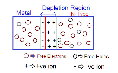
- In the unbiased condition, there is no external voltage applied to the Schottky diode.
- Free electrons from the n-type semiconductor naturally migrate toward the metal contact due to the difference in energy levels.
- This migration of electrons creates a charge imbalance at the junction.
- As a result, a depletion region forms near the metal-semiconductor interface.
- This region acts as a potential barrier, known as the Schottky barrier.
- The height of the Schottky barrier determines how easily electrons can cross the junction on applying external voltage.
Forward Bias Condition
- When the diode is forward biased (positive voltage on the metal side), electrons from the n-type semiconductor move toward the metal.
- Since there are plenty of electrons in the n-type material and the metal can easily absorb them, current flows quickly with very little resistance.
- The barrier potential is low, so the forward voltage drop is only about 0.2 to 0.4 volts.
Reverse Bias Condition
- When reverse biased, the metal tries to push electrons back into the n-type region.
- A depletion region forms at the junction, preventing current flow.
- Only a tiny leakage current flows until breakdown voltage is reached.
Key Features of Working
- No charge storage (unlike p-n junctions), which means very fast switching.
- Low forward voltage drop, reducing power loss in high-efficiency circuits.
V-I Characteristics of Schottky Diode
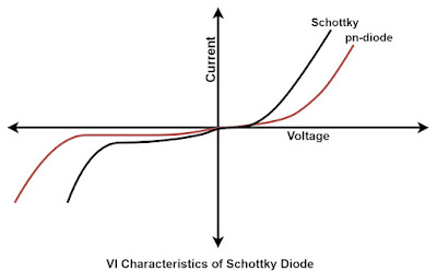
- The forward voltage drop is very low.
- The forward voltage drop ranges from 0.3 volts to 0.5 volts.
- The forward voltage drop increases with the increase of T N-type semiconductor concentration.
- TV-I characteristics are steeper due to a higher concentration of majority carriers
Difference Between Schottky Diode and PN Junction Diode
The surface barrier diode uses a metal-semiconductor junction, whereas the PN junction diode uses a P-type and N-type semiconductor.
The following table highlights the key differences between the two types of diodes:
| Feature | Schottky Diode | PN Junction Diode |
| Forward Voltage Drop | 0.2–0.3 V | 0.6–0.7 V |
| Switching Speed | Very High | Moderate |
| Junction Type | Metal-Semiconductor | P-N Semiconductor |
| Carrier Type | Majority | Majority + Minority |
| Applications | RF, Power circuits | General rectification |
Why Schottky Diode better than Germanium Diode
The forward voltage drop of the Schottky diode is 0.3 volts, similar to that of the germanium P-N junction diode. However, germanium diodes are rarely used because their switching speed is very low.
In the P-N junction diode, the conduction takes place through the majority carriers. However, if the minority carrier injects into the region, it is difficult to remove these charge carriers, and because of these stored charges, the device takes more time to go into the off state.
The turn-off time of the device increases when the charges stores in the depletion region. The turn-off time of the Schottky diode is very low, and this feature makes it suitable for high-frequency applications.
To improve switching speed and avoid saturation in BJTs, designers place a Schottky diode between the collector and base. This configuration forms the foundation of Schottky TTL logic circuits.
Applications of Schottky Diode
- Voltage clamping applications and prevention of transistor saturation
- Power rectifiers in switching power supplies due to low forward voltage drop and high efficiency
- Freewheeling diodes in motor control circuits to protect against voltage spikes
- Reverse current protection in battery-powered systems to prevent backflow of current
- Logic circuits in Schottky TTL families for fast switching
- Solar cell systems to minimize power loss from the photovoltaic output
- Voltage regulation and power OR-ing circuits to manage multiple power sources
- High-speed digital circuits requiring fast response times
Advantages of Schottky Diode
- Low turn-on voltage: The turn-on voltage for this diode is between 0.2 and 0.3 volts. This reduces power loss and improves efficiency in low-voltage circuits.
- Fast recovery time: A fast recovery time results from the minimal stored charge, making the diode suitable for high-speed switching applications such as digital logic and power electronics.
- Low junction capacitance: Due to the metal-semiconductor (M-S) construction and small depletion region, these diodes exhibit very low capacitance, making them ideal for high-frequency circuits where capacitance must be minimized.
Disadvantages of Schottky Diode
- One key drawback is its high reverse saturation current, which can lead to increased leakage current under reverse bias. This makes it less suitable for high reverse voltage applications compared to standard PN junction diodes.
Related Articles: